Layout method for PCB (Printed Circuit Board) mounted with BGA (Ball Grid Array) chip and PCB prepared by applying same

A chip and mounting technology, applied in the field of electronic circuits, can solve the problems of increasing the difficulty of PCB layout layout and wiring, increasing the development cycle and production cycle of electronic equipment, and large distribution density, so as to shorten the development and processing cycle, and shorten the development and production time , the effect of reducing difficulty

Active Publication Date: 2014-01-08
QINGDAO GOERTEK
View PDF4 Cites 2 Cited by
  • Summary
  • Abstract
  • Description
  • Claims
  • Application Information

AI Technical Summary

Problems solved by technology

However, the BGA chip has a large number of pins, and most of them are distributed in the bottom of the chip in the form of an array, and the distribution density is high, which increases the difficulty of PCB layout (layout and wiring) for mounting BGA chips, making the mounting of BGA chips difficult. The PCB will consume a lot of time whether it is in the design stage or the processing stage, which will increase the development cycle and production cycle of electronic equipment.

Method used


Image

  • Layout method for PCB (Printed Circuit Board) mounted with BGA (Ball Grid Array) chip and PCB prepared by applying same
  • Layout method for PCB (Printed Circuit Board) mounted with BGA (Ball Grid Array) chip and PCB prepared by applying same
  • Layout method for PCB (Printed Circuit Board) mounted with BGA (Ball Grid Array) chip and PCB prepared by applying same

Examples


Embodiment Construction

[0022] Below in conjunction with accompanying drawing and embodiment, further elaborate the present invention.

[0023] A PCB layout method with a BGA chip mounted thereon, comprising the following steps:

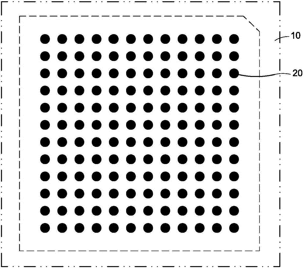
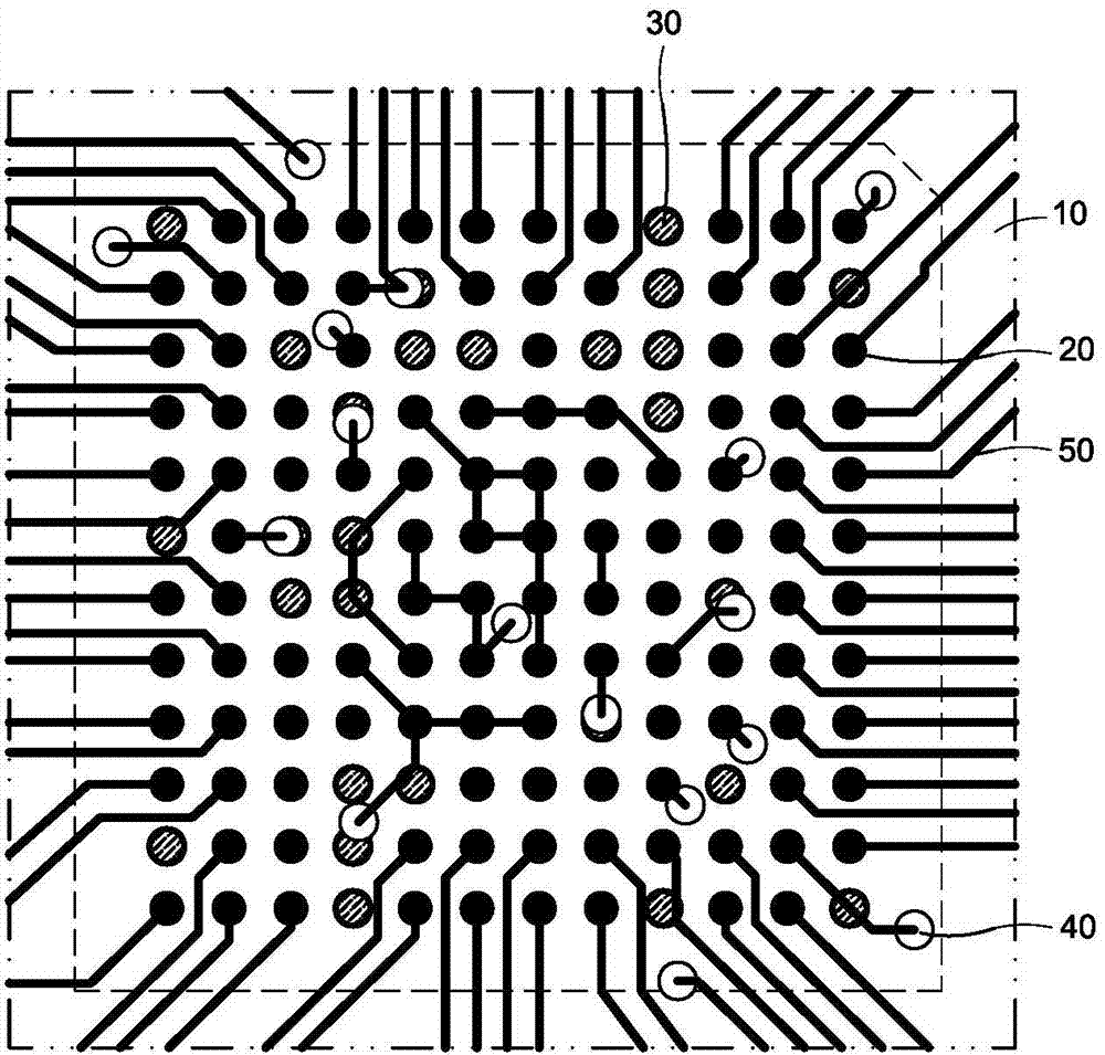
[0024] S1. Provide a PCB to be mounted with a BGA chip, the PCB is provided with solder joints corresponding to the pins of the BGA chip;

[0025] S2. Confirming that the NC pins of the BGA chip and / or function unused pins correspond to the positions of the solder joints on the PCB;

[0026] S3. Cover the solder joints corresponding to the NC pins of the BGA chip and / or functional unused pins with insulating ink;

[0027] S4. Arranging wires or making metallized through holes in the insulating ink coverage area according to functional requirements.

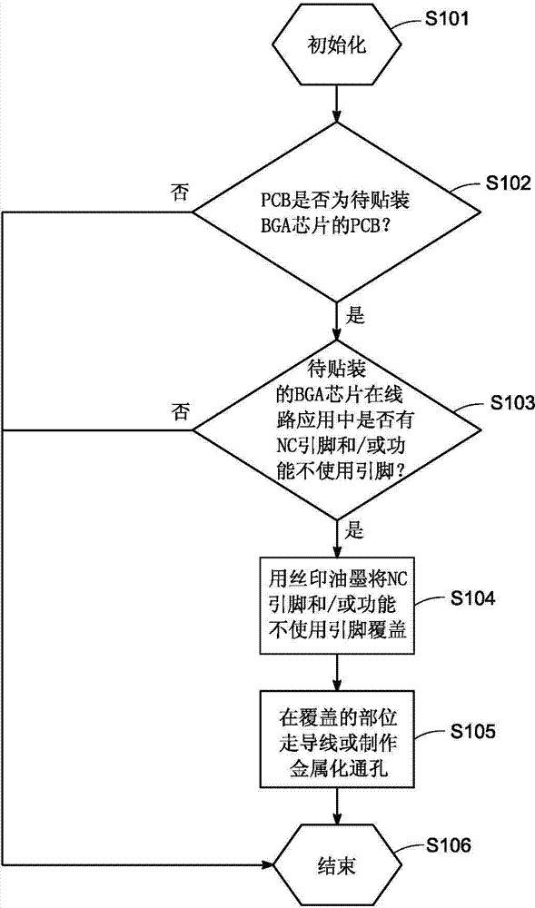
[0028] The specific program flow of the above method is as follows: image 3 Shown:

[0029] The program starts at step S101, performs device initialization at step S101, and enters step S102 after device initialization is ...


PUM


Abstract

The invention discloses a layout method for a PCB (Printed Circuit Board) mounted with a BGA (Ball Grid Array) chip and a PCB prepared by applying the same and relates to the technical field of an electronic circuit. The layout method comprises the following steps: S1, providing a PCB to be mounted with the BGA chip, wherein the PCB is provided with welding spots corresponding to pins of the BGA chip; S2, confirming the positions of the welding spots on the PCB, which correspond to an NC (Not Component) pin and / or a function nonuse pin; S3, covering the welding spots corresponding to the NC pin and / or the function nonuse pin of the BGA chip with insulation ink; and S4, according to functional requirements, wiring or forming metalized through holes in a coverage region of the insulation ink. The invention solves the technical problem of high layout difficulty of the PCB mounted with the GBA chip in the prior art. According to the invention, the layout difficulty of the PCB mounted with the GBA chip is reduced to the greatest extent and development and processing periods of the PCB mounted with the GBA chip are shortened.

Description

technical field [0001] The invention relates to the technical field of electronic circuits, in particular to a PCB layout method on which a BGA chip is mounted and a PCB prepared by applying the method. Background technique [0002] BGA (Ball Grid Array) is a packaging method for integrated circuits using organic carrier boards. BGA chips are chips that are packaged in BGA. The pins are not distributed around the chip, but on the bottom of the package. Compared with QFP (Plastic Quad Flat Package) packaged chips, it can maintain more package capacity under the same package size. At present, BGA chips are widely used in highly integrated electronic products, such as north and south bridge chips of computer motherboards, high-end graphics chips, and even some chips of printers and hard disks. [0003] With the development of science and technology, the volume of electronic equipment is constantly shrinking, and the PCB (Printed Circuit Board) in electronic equipment is also b...

Claims


Application Information

Patent Timeline
Patent Type & Authority Applications(China)
IPC IPC(8): H01L21/60H01L21/48H05K3/28
CPCH05K3/28
Inventor 邓雪冰
Owner QINGDAO GOERTEK
Why Eureka
Try Eureka