Light-emitting diode (LED) display screen and packaging method thereof

A technology of LED display screen and packaging method, which is applied in the direction of identification devices, instruments, electrical components, etc. It can solve problems such as short circuit, easy convergence of light-emitting areas, affecting product yield and production capacity, etc., to achieve clear display effect and reduce mixed light phenomenon or the effect of infiltration

Active Publication Date: 2014-01-22
GUANGDONG VTRON TECH CO LTD
View PDF12 Cites 41 Cited by
  • Summary
  • Abstract
  • Description
  • Claims
  • Application Information

AI Technical Summary

Problems solved by technology

On the one hand, although the resolution of SMD LED display screens has been greatly improved at present, there is still room for improvement in the resolution of LED display screens due to the requirements for high-resolution indoor display screens.
However, as the size of small-sized SMD LEDs decreases, there are technical difficulties in the packaging process and the subsequent display screen placement process.
For example, small-sized SMD LEDs involve the subsequent cutting process and require high precision. Due to the small size and small pads in the patch, it is easy to cause a short circuit when printing solder, and it is also more difficult for the suction nozzle to grab the device, which affects the quality of the product. Yield and production capacity; on the other hand, the directionality of SMD LED light emission makes its light-emitting areas easy to converge, causing glare and glare and mixed light problems are more likely, especially for indoor display screens, this shortcoming is more obvious
In addition, small-size SMD LEDs have inconsistent heights for each device during placement, which can easily lead to consistency problems in product optical performance

Method used


Image

  • Light-emitting diode (LED) display screen and packaging method thereof
  • Light-emitting diode (LED) display screen and packaging method thereof
  • Light-emitting diode (LED) display screen and packaging method thereof

Examples


Embodiment Construction

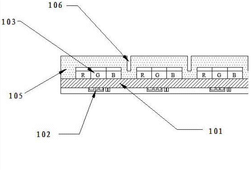
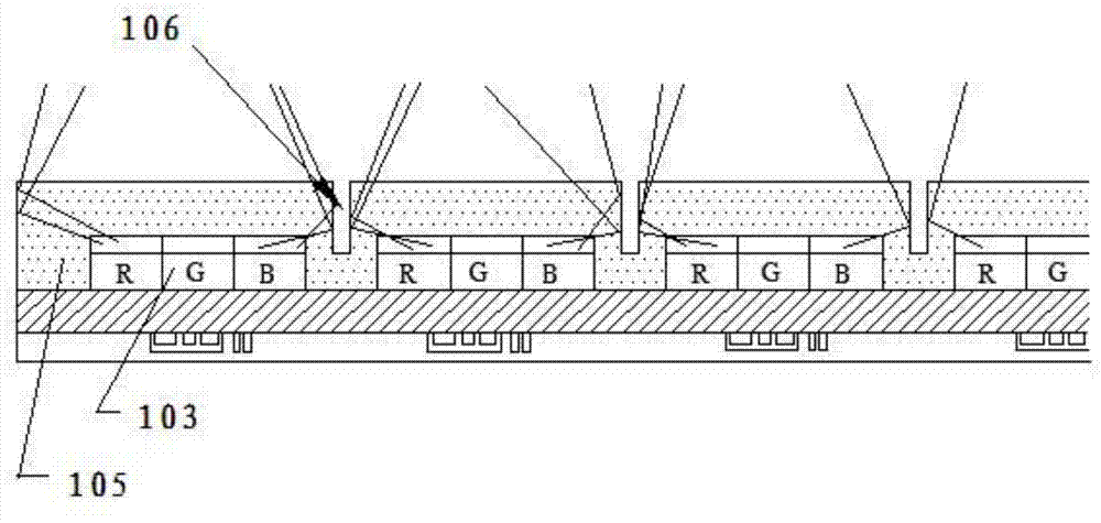
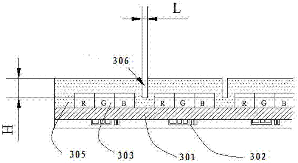
[0048] The embodiment of the present invention provides an LED display screen, which can further reduce the distance between each group of RGB LED chips, improve the resolution of the display screen, and effectively solve the problem of confusion between RGB LED chips. Light phenomenon, thereby effectively improving the display effect.

[0049] Combine the following figure 1 The specific structure of an LED display screen provided by the embodiment of the present invention is described in detail;

[0050] Such as figure 1 As shown, the LED display screen specifically includes a COB board 101, at least one driver chip 102 and an LED lamp module.

[0051] Its specific structure is that the driver chip 102 is arranged on the back of the COB board 101 , and the LED lamp module is arranged on the front of the COB board 101 .

[0052]Specifically, the LED lamp module includes at least one set of RGB LED chips 103, and the set of RGB LED chips 103 is arranged in a straight line; ...


PUM


Abstract

An embodiment of the invention discloses a light-emitting diode (LED) display screen and a packaging method thereof. The LED display screen comprises a COB (chip on board) board, at least one driving chip and an LED lamp module. The driving chips are arranged on the back of the COB board, the LED lamp module is arranged on the front of the COB board and comprises at least one group of RGB (red green blue) LED chips, the RGB LED chips are covered with packaging glue, and slits are arranged in the packaging glue between the RGB LED chips. Light mixing or invasion of light emitted by every group of RGB LED chips can be reduced while optical consistency of the LED display screen can be improved and glare can be reduced.

Description

technical field [0001] The invention relates to the technical field of LED display screens, in particular to an LED display screen and a packaging method thereof. Background technique [0002] In recent years, LED indoor display screens have developed rapidly, and products are increasingly developing in the direction of high-density, small dot pitch and full-color high-resolution. At present, most of the full-color LED displays with higher density and smaller dot pitch are used in surface mount LED packaging, that is, SMD LED. However, when large-sized SMD LEDs are packaged into a display screen, due to the ubiquity of dark areas, the division between pixels of the display screen is obvious, resulting in a rough display screen with strong graininess and not fine enough. With the development of surface mount technology (SMT), the size of SMD LEDs has become smaller and smaller, which has greatly reduced the dot pitch of full-color LED displays, and displays with pixels small...

Claims


Application Information

Patent Timeline
Patent Type & Authority Applications(China)
IPC IPC(8): G09F9/33H01L33/54H01L33/58H01L33/60H01L33/48
Inventor 李春辉胡新喜董萌吴曼
Owner GUANGDONG VTRON TECH CO LTD
Why Eureka
Try Eureka