select device

A selective device, semi-conductive technology, applied in the direction of digital memory information, diodes, instruments, etc., can solve the problems of increasing the leakage current of TFT semiconductor materials, poor interface characteristics, long processing time, etc.

Active Publication Date: 2018-01-30
MICRON TECH INC
View PDF3 Cites 0 Cited by
  • Summary
  • Abstract
  • Description
  • Claims
  • Application Information

AI Technical Summary

Problems solved by technology

[0005] However, SPC has disadvantages in that: the processing time is long; and there is a risk of substrate deformation caused by the long processing time and high temperature for annealing
ELC has disadvantages in that: expensive laser equipment is required; and interface characteristics between semiconductor material and gate insulating material are poor due to protrusions generated on the formed polycrystallized surface
MIC and MILC have the disadvantage that a large amount of crystallization-inducing metal remains on the crystalline polysilicon material to increase the leakage current of the semiconductor material of the TFT

Method used


Image

  • select device
  • select device
  • select device

Examples


Embodiment Construction

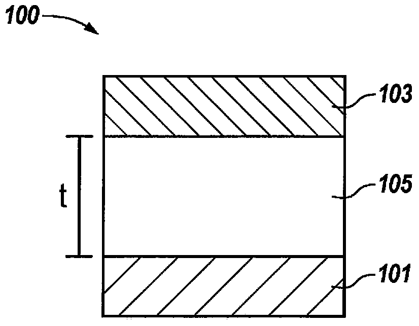
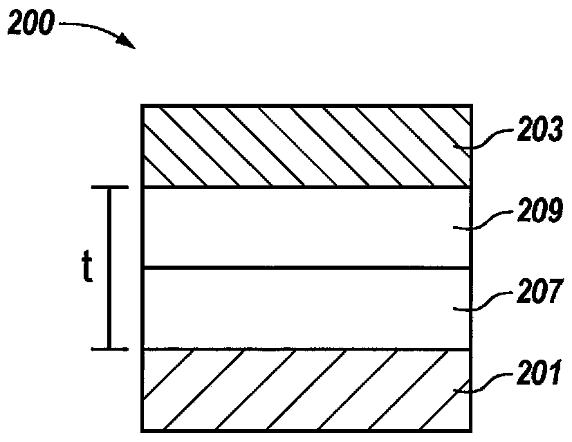
[0010] Methods, devices, and systems associated with selecting a device are described herein. The one or more selection devices may include at least one semiconductive stack of semiconductive material formed on the first electrode. The semiconducting stack can have approximately 700 Angstroms or less, and each of the at least one semiconducting material may have an associated bandgap of about 4 electron volts (eV) or less. A second electrode can be formed on the semiconducting stack.

[0011] Embodiments of the present invention may provide selection devices capable of supporting increased current densities over previous selection devices. In various embodiments, the structure of the selection device may include a semiconducting stack that can be tuned to accommodate different memory cell characteristics such as, for example, symmetric or asymmetric current versus voltage signatures. In one or more embodiments, select devices are provided that can withstand a large number ...


PUM


Abstract

The present invention provides methods, devices and systems for a selection device which may comprise at least one semiconductive stack of semiconductive material formed on a first electrode, wherein the semiconductive stack may have a thickness of about 700 Angstroms or less thickness. Each of the at least one semiconducting material can have an associated bandgap of about 4 electron volts (eV) or less and a second electrode can be formed on the semiconducting stack.

Description

technical field [0001] The present invention relates generally to semiconductor electronic devices and methods, and more particularly, the present invention relates to selection devices. Background technique [0002] In a computer or other electronic device, the memory device is usually provided as an internal semiconductor integrated circuit. There are many different types of memory, including volatile memory and nonvolatile memory. Volatile memory can require power to maintain its information and includes Random Access Memory (RAM), Dynamic Random Access Memory (DRAM) and Synchronous Dynamic Random Access Memory (SDRAM), among others. Non-volatile memory provides persistent information by retaining stored information when power is not applied and can include NAND flash memory, NOR flash memory, read-only memory (ROM), electronically erasable programmable ROM (EEPROM), erasable In addition to programmable ROM (EPROM), phase change random access memory (PCRAM), resistive r...

Claims


Application Information

Patent Timeline
Patent Type & Authority Patents(China)
IPC IPC(8): H01L21/328H01L29/72
CPCH01L27/1021H01L29/872H01L29/885H10B61/10H10B63/20H10N70/20H10N70/882H10N70/231H10N70/8836H10N70/011H10N70/8833G11C11/5678G11C13/0004G11C2213/71H10K19/202H01L29/72H01L21/18H10N70/826
Inventor D·V·尼马尔·拉马斯瓦米古尔特杰·S·桑胡
Owner MICRON TECH INC
Why Eureka
Try Eureka