Liquid crystal display panel, driving method thereof and liquid crystal displayer with liquid crystal display panel
A liquid crystal display panel and driving method technology, applied in static indicators, instruments, nonlinear optics, etc., can solve problems such as backlight waste, achieve energy saving and improve backlight utilization
- Summary
- Abstract
- Description
- Claims
- Application Information
AI Technical Summary
Problems solved by technology
Method used
Image
Examples
Embodiment 1
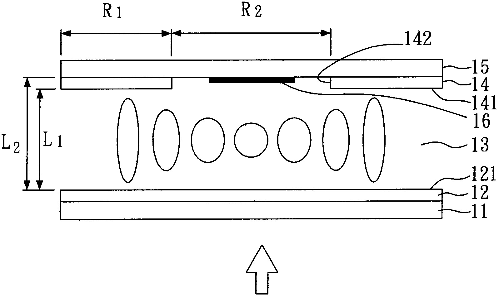
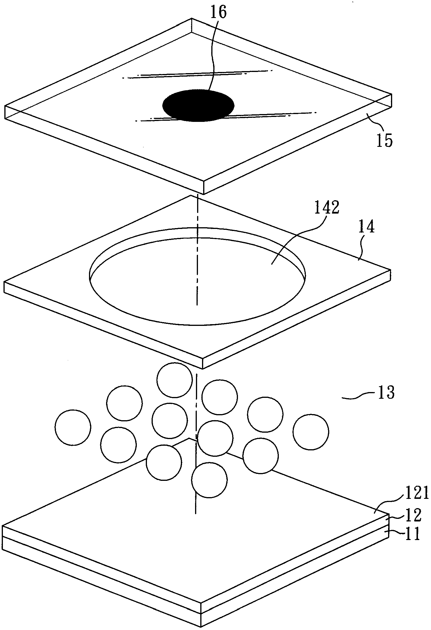
[0038] figure 1 It is a schematic cross-sectional view of the liquid crystal display panel of this embodiment after applying a bias voltage, figure 2 It is a three-dimensional exploded schematic view of the liquid crystal display panel of this embodiment before applying a bias voltage.
[0039] Please also refer to figure 1 and figure 2 , the liquid crystal display panel of the present embodiment comprises: a first substrate 11 is provided with a first electrode layer 12, and the first electrode layer 12 has a first surface 121; a second substrate 15, opposite to the first substrate 11 arranged in parallel, the second substrate 15 is provided with a second electrode layer 14, the second electrode layer 14 has a second surface 141, and the second surface 141 is corresponding to the first surface 121 of the first electrode layer 12; The blue phase liquid crystal layer 13 includes a blue phase liquid crystal, and the blue phase liquid crystal layer 13 is arranged between the...
Embodiment 2
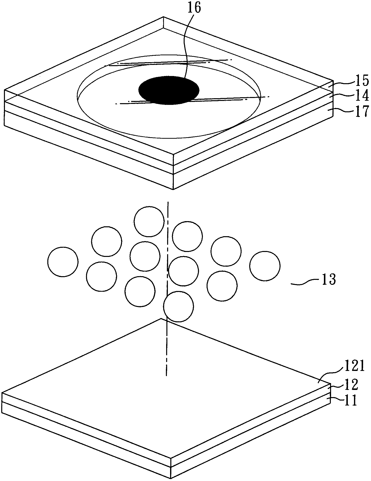
[0045] image 3 It is a schematic perspective view of the liquid crystal display panel of this embodiment before applying a bias voltage. Such as image 3 As shown, the structure and driving method of the liquid crystal display panel of the present embodiment are the same as Embodiment 1, except that a microlens array 17 is also provided below the second electrode layer 14 and relative to the first electrode layer 12; thus it can help Focusing of light passing through the blue phase liquid crystal layer 13 . In other embodiments, the microlens array can also be disposed between the second electrode layer 14 and the second substrate 15 , depending on design requirements.
Embodiment 3
[0047] Figure 4 It is a schematic cross-sectional view of the liquid crystal display panel of the present embodiment after a bias voltage is applied. Such as Figure 4 As shown, the structure and driving method of the liquid crystal display panel of this embodiment are the same as those of Embodiment 1, except that a dielectric layer 19 is also provided below the second electrode layer 14 and opposite to the first electrode layer 12 to help pass blue Focusing of the light rays of the phase liquid crystal layer 13. In addition, the liquid crystal display panel of this embodiment is not provided with the light-shielding area of Embodiment 1, but focuses the light passing through the blue-phase liquid crystal layer 13 on the black matrix of the color filter 18, and the black matrix achieves the effect of absorbing light. effect.
PUM
 Abstract
Description
Claims
Application Information


