Automatic visual detection method and device for Mura defects of thin film transistor liquid crystal display (TFT-LCD) process

An automatic detection and visual technology, applied in the direction of optical testing flaws/defects, optics, instruments, etc., can solve problems such as the difficulty of manual detection methods to meet product quality and production efficiency, the lack of uniform judgment standards for defect levels, and the increase of liquid crystal displays. Achieve the effect of avoiding a large number of floating-point operations, facilitating subsequent processing, and improving performance

Active Publication Date: 2014-02-05
苏州富鑫林光电科技有限公司
View PDF4 Cites 19 Cited by
  • Summary
  • Abstract
  • Description
  • Claims
  • Application Information

AI Technical Summary

Problems solved by technology

[0002] With the development of liquid crystal displays (LCDs) in the direction of large size, lightness, low power consumption, and high resolution, the size of glass substrates and related optical components is gradually increasing, and their thickness is decreasing, resulting in various realities of liquid crystal displays. The probability of un

Method used


Image

  • Automatic visual detection method and device for Mura defects of thin film transistor liquid crystal display (TFT-LCD) process
  • Automatic visual detection method and device for Mura defects of thin film transistor liquid crystal display (TFT-LCD) process
  • Automatic visual detection method and device for Mura defects of thin film transistor liquid crystal display (TFT-LCD) process

Examples


Embodiment Construction

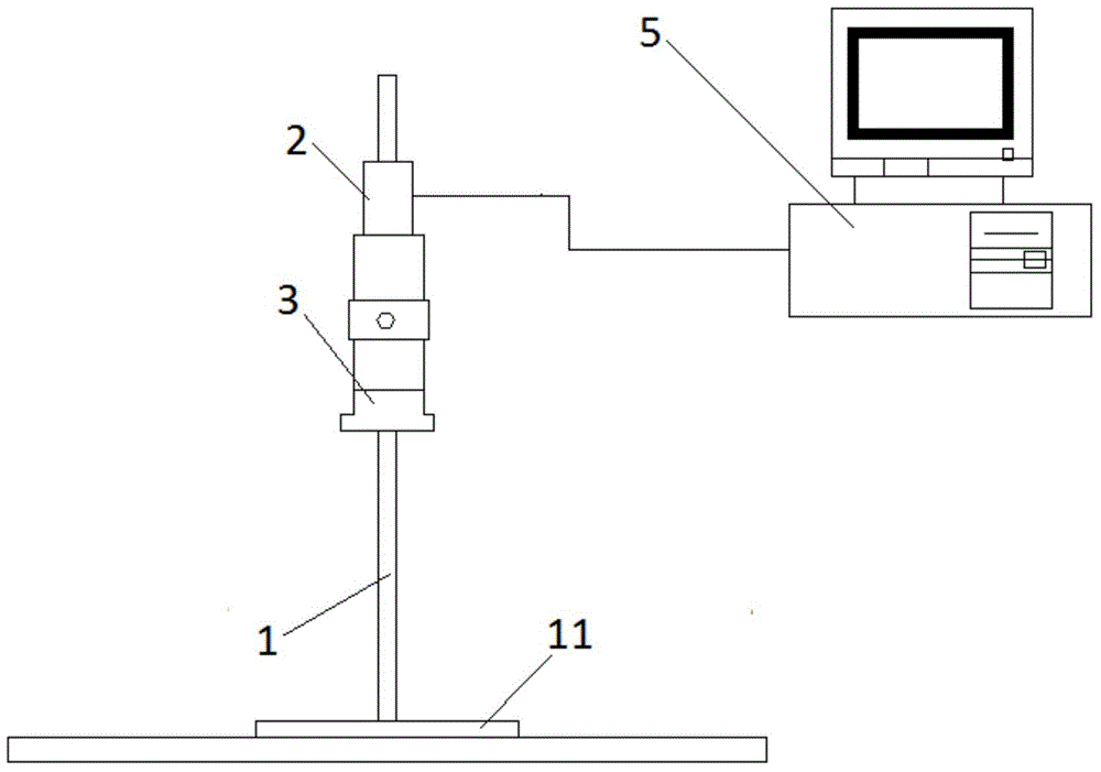
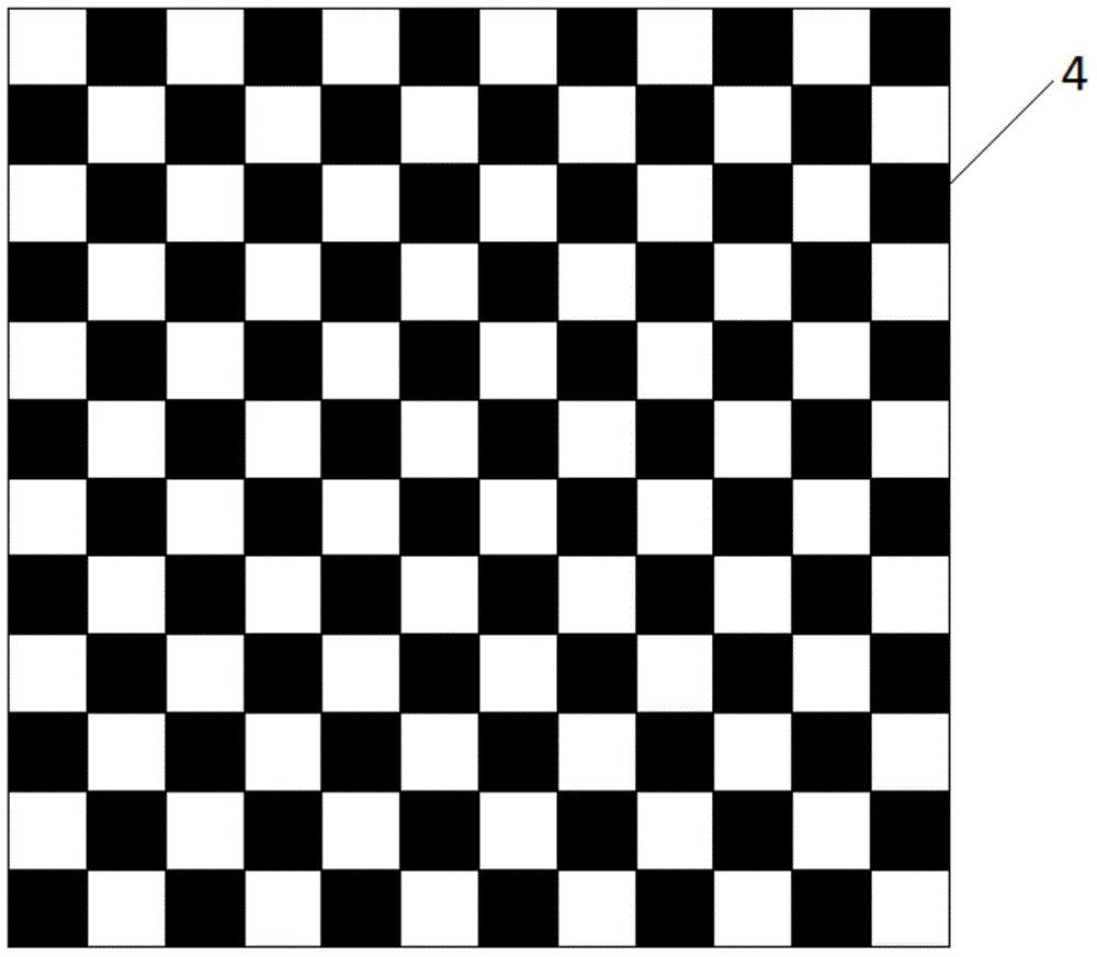
[0038] Refer to Figure 1-2 , The MURA vision automatic inspection device of the TFT-LCD process includes a fixing device 1, a CCD camera device 2, a lens 3, and a standard square angle Figure 4 And the computer 5, the fixing device 1 is equipped with a fixed jig 11 of the measured object, and the square angle standard Figure 4 Laying on the upper surface of the fixed fixture 11 of the measured object, the CCD camera device 2 is installed on the fixed device 1 and above the fixed fixture 11 of the measured object, the lens 3 is set on the CCD camera device 2, and the CCD camera device 2 passes The connecting line is connected with the computing card set on the computer 5.

[0039] Among them, the computer 5 is provided with a low-pass filter based on discrete Fourier change and a GPU.

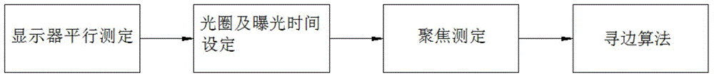
[0040] Refer to Figure 3-7 , A MURA vision automatic inspection method for TFT-LCD manufacturing process, which includes

[0041] Image preparation process:

[0042] 1) Place the object to be teste...


PUM


Abstract

The invention discloses an automatic visual detection device for Mura defects of a thin film transistor liquid crystal display (TFT-LCD) process. The device comprises a fixing device, a charge coupled device (CCD) photographic device, a lens and a square angle standard graph, wherein the fixing device is provided with a detected object fixing tool; the square angle standard graph is laid on the upper surface of the detected object fixing tool; the CCD photographic device is arranged on the fixing device and is arranged above the detected object fixing tool; the lens is arranged on the CCD photographic device; the CCD photographic device is connected with an operation card, which is arranged on a computer, through a connecting line. Different types and sizes of the Mura defects of the TFT-LCD process can be indentified by operating different environments in a compatible manner, intelligent detection is realized, and the labor cost is reduced.

Description

technical field [0001] The invention relates to a detection device and method of a flat panel display, in particular to a MURA visual automatic detection method and device of a TFT-LCD manufacturing process. Background technique [0002] With the development of liquid crystal displays (LCDs) in the direction of large size, light weight, low power consumption, and high resolution, the size of glass substrates and related optical components is gradually increasing, and their thickness is decreasing, resulting in various realities of liquid crystal displays. The probability of uneven defects (Mura) is greatly increased. The traditional human eye defect detection method is seriously affected by human subjective factors and the external environment. There is no uniform judgment standard for defect levels. It is difficult to make manual detection methods meet the requirements of product quality and production efficiency. Therefore, it is an urgent requirement for the development ...

Claims


Application Information

Patent Timeline
IPC IPC(8): G01N21/94G02F1/13
Inventor 许照林冯海丁吴全玉
Owner 苏州富鑫林光电科技有限公司
Why Eureka
Try Eureka