A shunt component of a printed circuit board

A technology for printed circuit boards and shunt components, which is applied to printed circuit components, resistive elements adjusted by short-circuiting different numbers of resistive elements, and contact parts. Low-level problems, to achieve the effect of increasing the average output, simplifying the process, and simplifying the structure

Active Publication Date: 2017-01-11
REPOWER TECH CO LTD
View PDF5 Cites 0 Cited by
  • Summary
  • Abstract
  • Description
  • Claims
  • Application Information

AI Technical Summary

Problems solved by technology

[0005] The purpose of the embodiment of the present invention is to provide a shunt element of a printed circuit board, aiming at solving the problem that the shunt element of a printed circuit board provided by the prior art is welded by manganese copper and red copper, and the shunt element needs to be adjusted. resistance, which makes the processing time long, the average output is low, the production cost is high, and the resistance value cannot be increased

Method used


Image

  • A shunt component of a printed circuit board
  • A shunt component of a printed circuit board
  • A shunt component of a printed circuit board

Examples


specific Embodiment approach

[0021] In order to make the objectives, technical solutions and advantages of the present invention clearer, the following further describes the present invention in detail with reference to the accompanying drawings and embodiments. It should be understood that the specific embodiments described herein are only used to explain the present invention, but not to limit the present invention.

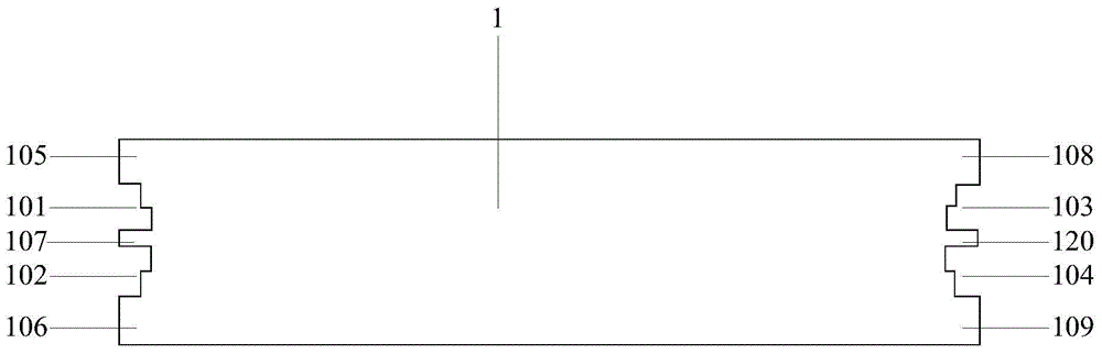
[0022] Aiming at the problems existing in the prior art, the present invention proposes a shunt element of a printed circuit board. The shunt element is formed by bending a strip of metal sheet, and at least one notch is opened on the opposite first end and second end of the strip metal sheet, so that the first end is divided into at least one first-type pin and at least A second-type pin, the second end is divided into at least one third-type pin and at least one fourth-type pin, and the width of the first-type pin is greater than the width of the second-type pin, and the third-type lead Th...

Embodiment 1

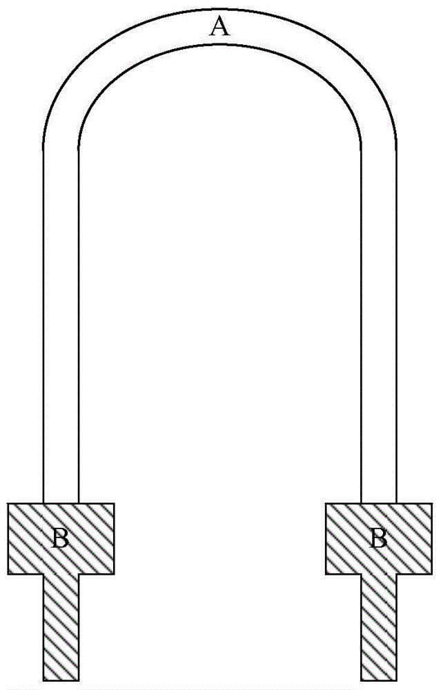
[0024] The first embodiment of the present invention proposes a shunt element of a printed circuit board, the shunt element adopts a central sampling structure, such as figure 2 It is an extended schematic view of the shunt element of the printed circuit board provided in the first embodiment of the present invention, image 3 It is a three-dimensional schematic diagram of the shunt element of the printed circuit board provided by the first embodiment of the present invention. The three-dimensional schematic diagram of the three-dimensional structure is an example of a strip metal sheet bent into an m shape. Of course, it can also be bent into an n according to the actual situation of the printed circuit board Shape or other arbitrary shapes. For ease of illustration, figure 2 versus image 3 Only the parts related to Embodiment 1 of the present invention are shown.

[0025] In detail, combined figure 2 with image 3 As shown, the shunt element of the printed circuit board prov...

Embodiment 2

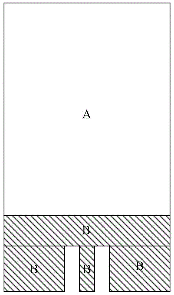
[0034] The second embodiment of the present invention proposes a shunt element of a printed circuit board, which adopts a cross-average sampling structure, such as Image 6 It is an extended schematic diagram of the shunt element of the printed circuit board provided in the second embodiment of the present invention, Figure 7 It is a three-dimensional schematic diagram of the shunt element of the printed circuit board provided in the second embodiment of the present invention. The three-dimensional schematic diagram of the three-dimensional structure is an example of a strip metal sheet bent into an m shape. Of course, it can also be bent into an n according to the actual situation of the printed circuit board. Shape or other arbitrary shapes. For ease of illustration, Image 6 versus Figure 7 Only the parts related to the second embodiment of the present invention are shown.

[0035] In detail, combined Image 6 with Figure 7 As shown, the shunt element of the printed circuit ...


PUM


Abstract

The invention belongs to the technical field of electric parameter measurement, and provides a shunting element for a printed circuit board. The shunting element is formed by bending a strip-type metal sheet, wherein at least one notch is formed in each of the opposite first and second ends of the strip-type metal sheet, so that the first end is divided into at least one first-type pin and at least one second-type pin, and the second end is divided into at least one third-type pin and at least one fourth-type pin; the width of the first-type pin is greater than that of the second-type pin, and the width of the third-type pin is greater than that of the fourth-type pin. The shunting element is integrally machined by using the strip-type metal sheets, and is simple in structure; the resistance of a finished product is not required to be regulated, so that manufacturing procedures are simplified; at the same time, a conventional terminal sheet part is rreduced, so that a resistance value can be increased or decreased according to actual needs, and the shunting element is high in flexibility; moreover, a welding procedure is not required, so that the shunting element has the advantage of small temperature drift.

Description

Technical field [0001] The invention belongs to the technical field of electrical parameter measurement, and particularly relates to a shunt element of a printed circuit board. Background technique [0002] The shunt component is a device that is widely used in communication systems, electronic complete machines, automatic control power supplies and other circuits to achieve current limiting and current sharing sampling detection. It generates voltage across the resistor when the DC current passes through the resistor. The principle is made. [0003] Figure 1a Shows a side view of a shunt element applied on a printed circuit board in the prior art, Figure 1b Yes Figure 1a The front view, taking the n-shaped structure as an example. The shunt element includes a resistor piece and an end piece for connecting to the printed circuit board. The resistor piece is shown in the unshaded part A, and the end piece is shown in the shaded part B. Among them, the resistance piece is made of ...

Claims


Application Information

Patent Timeline
Patent Type & Authority Patents(China)
IPC IPC(8): H01C10/06H05K1/02H01R13/02
Inventor 毛广甫
Owner REPOWER TECH CO LTD
Why Eureka
Try Eureka