
MEMS device with silicon-based piezoresistive sensor

A piezoresistive, sensor technology

Active Publication Date: 2021-07-30
SHENZHEN GRADUATE SCHOOL TSINGHUA UNIV
View PDF5 Cites 0 Cited by
  • Summary
  • Abstract
  • Description
  • Claims
  • Application Information

AI Technical Summary

Problems solved by technology

However, the silicon-based piezoresistive angle sensor based on the Wheatstone bridge structure requires high photolithography alignment accuracy at the four terminals in the micro-nano-fabrication process, which may easily lead to the resistance of the four resistors in the Wheatstone bridge structure. Inconsistency, which further leads to deviation of the sensing signal

Method used


Image

  • MEMS device with silicon-based piezoresistive sensor
  • MEMS device with silicon-based piezoresistive sensor
  • MEMS device with silicon-based piezoresistive sensor

Examples


Embodiment Construction

[0032] Embodiments of the present invention will be described in detail below. It should be emphasized that the following description is only exemplary and not intended to limit the scope of the invention and its application.

[0033] It should be noted that when an element is referred to as being “fixed” or “disposed on” another element, it may be directly on the other element or be indirectly on the other element. When an element is referred to as being "connected to" another element, it can be directly connected to the other element or indirectly connected to the other element. In addition, the connection can be used for fixation as well as for coupling or communication.

[0034] It is to be understood that the terms "length", "width", "top", "bottom", "front", "rear", "left", "right", "vertical", "horizontal", "top" , "bottom", "inner", "outer" and other indicated orientations or positional relationships are based on the orientations or positional relationships shown in ...


PUM

PropertyMeasurementUnit
sizeaaaaaaaaaa

Abstract

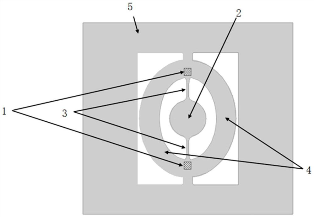
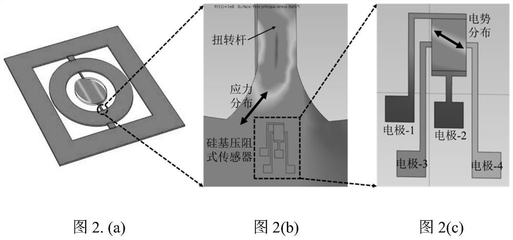
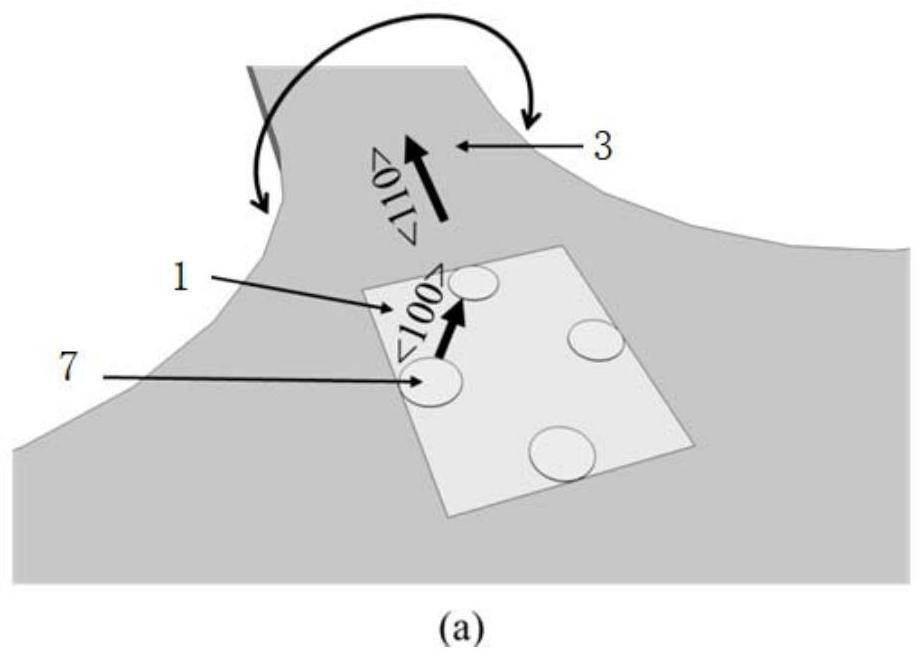
An MEMS device with a silicon-based piezoresistive sensor comprises an MEMS galvanometer and the silicon-based piezoresistive sensor, the MEMS galvanometer comprises a reflecting mirror, two torsion rods and an MEMS driver, the reflecting mirror is fixed on the MEMS driver through the two torsion rods, the silicon-based piezoresistive sensor is arranged based on a Wheatstone bridge structure and is used for sensing the torsion angle of the reflecting mirror, the silicon-based piezoresistive sensor is of a square or rectangular structure and is placed near the fixed end of the torsion rod, and the gradient direction of the electric potential energy generated by the silicon-based piezoresistive sensor under the action of the torsion shear stress of the reflecting mirror is consistent with the gradient direction of the stress. According to the MEMS device, the requirement for high precision of photoetching alignment in the micro-nano technology can be lowered, the overall structure size of the MEMS galvanometer is small and integrated, and the overall device cost is lowered.

Description

technical field [0001] The invention relates to MEMS devices, in particular to a MEMS device with a silicon-based piezoresistive sensor. Background technique [0002] With the rapid development of micro-nano processing technology, MEMS (Microelectromechanical systems) devices have been widely used in industrial production, automobiles, mobile phones, security and other industries based on their advantages of small integration, low power consumption, light weight, and easy mass production. aspect. Among them, MEMS vibrating mirror is an important development and application direction. MEMS technology is used to integrate the low-light mirror and MEMS driver on the MEMS device, which can chip the traditional mirror surface rotation device, and has high reliability, low cost, and small size. , easy integration and other advantages, mainly used in lidar, machine vision, face recognition, virtual / augmented reality (VR / AR), micro-projector (Micro-projector) and other aspects. Th...

Claims


Application Information

Patent Timeline
Patent Type & Authority Applications(China)
IPC IPC(8): B81B7/02G02B26/08
CPCB81B7/02G02B26/0833B81B2201/042
Inventor 薛高鹏李星辉王晓浩
Owner SHENZHEN GRADUATE SCHOOL TSINGHUA UNIV
Learn More