Pixel structure of a high light sensitivity CMOS image sensor

A technology of image sensor and pixel structure, applied in image communication, TV, color TV components and other directions, can solve problems such as increasing complexity, and achieve the effect of improving light sensitivity and signal-to-noise ratio

Active Publication Date: 2019-07-19
SHANGHAI INTEGRATED CIRCUIT RES & DEV CENT
View PDF6 Cites 0 Cited by
  • Summary
  • Abstract
  • Description
  • Claims
  • Application Information

AI Technical Summary

Problems solved by technology

This method needs to use at least two independent signal lines to output optical signals, because the shared readout circuit needs to output the signals on each pixel unit separately, and the same readout circuit also needs to be used multiple times, which increases the complexity

Method used


Image

  • Pixel structure of a high light sensitivity CMOS image sensor
  • Pixel structure of a high light sensitivity CMOS image sensor
  • Pixel structure of a high light sensitivity CMOS image sensor

Examples


Embodiment Construction

[0017] In order to make the content of the present invention clearer and easier to understand, the content of the present invention will be further described below in conjunction with the accompanying drawings. Of course, the present invention is not limited to this specific embodiment, and general replacements known to those skilled in the art are also covered within the protection scope of the present invention. In addition, the present invention is described in detail by means of schematic diagrams. When describing the examples of the present invention in detail, for the sake of illustration, the schematic diagrams are not partially enlarged according to the general scale, which should not be used as a limitation of the present invention.

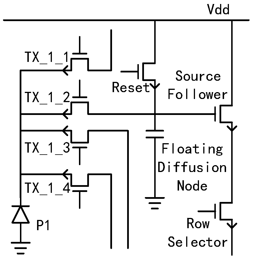
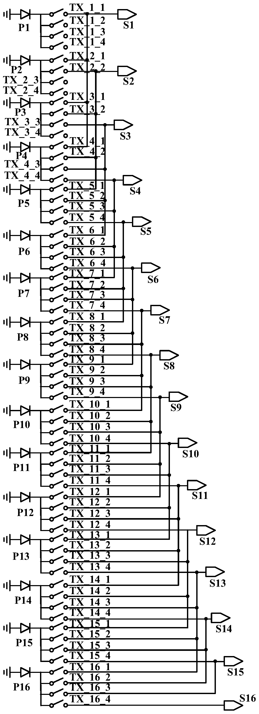
[0018] The present invention provides a high light sensitivity CMOS image sensor pixel structure, which includes M pixel units and a control unit, each pixel unit includes a photosensitive unit and a readout circuit, wherein the photosens...


PUM


Abstract

The invention discloses a high-luminous sensitivity CMOS image sensor pixel structure which comprises M pixel units and a control unit. Each pixel unit comprise a light sensing unit and a reading circuit, wherein the light sensing unit comprises a photodiode and N pass transistors; one of the N pass transistors of each pixel unit is connected with the reading circuit of the pixel unit, and the remaining N-1 pass transistors of each of at least M-N+1 pixel units are connected with the reading circuits of the other N-1 pixel units respectively; the reading circuit of each of at least M-N+1 pixel units is connected with one pass transistor of the pixel unit and the N-1 pass transistors of the other different pixel units, so that photoproduction signals of the N pixel units are read at one time; the control unit controls the M reading circuits to read the signals according to a specified order, so that the photoproduction signals of at least M-N+1 pixel units are read for N times in sequence. The high-luminous sensitivity CMOS image sensor pixel structure can increase the luminous sensitivity and signal to noise ratio on the condition of low illumination.

Description

technical field [0001] The invention relates to the field of semiconductor integrated circuits, in particular to a pixel structure of a CMOS image sensor with high light sensitivity. Background technique [0002] CMOS image sensors, due to their continuously improving optical and electrical properties, have been widely used in mobile phones, digital cameras, electron microscopes, etc., consumer electronics and scientific applications. Especially in the case of poor lighting conditions, the need to still achieve high-definition image capture is becoming a trend in these applications. Therefore, there are more urgent requirements for high-performance image sensors, especially to achieve high light sensitivity and signal-to-noise ratio of image sensors under low light. [0003] In the current CMOS image sensor technology, the signal-to-noise ratio of the image is improved by reducing the readout noise of the readout circuit, or by increasing the photosensitive area filling rat...

Claims


Application Information

Patent Timeline
Patent Type & Authority Patents(China)
IPC IPC(8): H04N5/374
Inventor 谈佳明李琛温建新
Owner SHANGHAI INTEGRATED CIRCUIT RES & DEV CENT
Why Eureka
Try Eureka