Fast recovery diode chip with low-concentration doped emitter region and its manufacturing method

A manufacturing method and emission area technology, applied in semiconductor/solid-state device manufacturing, electrical components, circuits, etc., can solve problems such as high manufacturing cost and complicated process flow, and achieve self-built potential difference reduction, low reverse recovery peak current, Effect of fast-acting switching speed

Active Publication Date: 2016-09-21
STATE GRID CORP OF CHINA +2
View PDF3 Cites 2 Cited by
  • Summary
  • Abstract
  • Description
  • Claims
  • Application Information

AI Technical Summary

Problems solved by technology

[0003] In order to pursue faster switching characteristics and better recovery softness, traditional high-power fast recovery diodes usually adopt life-controlled manufacturing and processing technology. The above-mentioned manufacturing technology has a complicated process and high manufacturing costs.

Method used


Image

  • Fast recovery diode chip with low-concentration doped emitter region and its manufacturing method
  • Fast recovery diode chip with low-concentration doped emitter region and its manufacturing method

Examples


Embodiment Construction

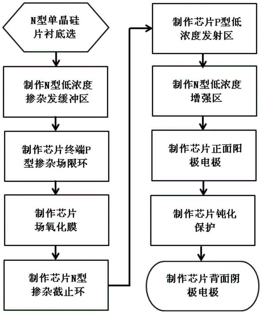
[0044] The specific implementation manners of the present invention will be further described in detail below in conjunction with the accompanying drawings.

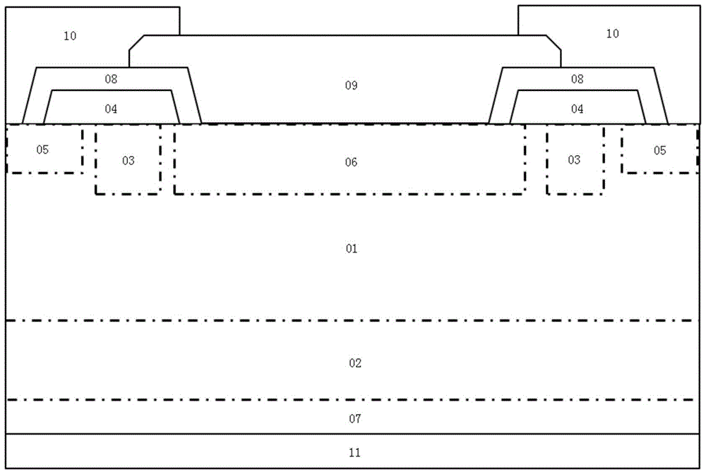
[0045] The schematic diagram of the structure of the low-concentration doped emitter region of the high-voltage fast recovery diode provided by the present invention is as follows: figure 1 As shown, the diode includes a metal cathode 11 and a metal anode 09, a P-type doped layer, an N-type doped layer, and an N-type substrate 01 disposed between the P-type doped layer and the N-type doped layer, The structure of the field oxide layer 04 and the passivation protection layer 10, the P-type doped layer is a low-concentration anode P-type doped emitter region 06, and the N-type doped layer includes a low-concentration cathode N-type buffer connected in sequence The doped region 02 and the low-concentration cathode N-type enhanced doped region 07, the metal cathode 11 is arranged on the bottom surface of the N-type substrate...


PUM


Abstract

The invention relates to a power device and a manufacturing method of the power device, in particular to a fast recovery diode chip of a low-concentration doped emitter region and a manufacturing method of the fast recovery diode chip of the low-concentration doped emitter region. The fast recovery diode chip of the low-concentration doped emitter region comprises a metal cathode, a metal anode, a P-type doped layer, an N-type doped layer, an N-type substrate arranged between the P-type doped layer and the N-type doped layer, field oxide layers and passivation protective layer structures, wherein the metal anode is a low-concentration P-type doped region, the metal cathode is a low-concentration N-type buffer doped region and a low-concentration N-type reinforced doped region, the special manufacturing mode of injection doped of the reverse side is formed through an obverse side protection technology, and a device structure is formed through the special manufacturing mode of injection doped of the reverse side. According to the fast recovery diode chip of the low-concentration doped emitter region and the manufacturing method of the fast recovery diode chip of the low-concentration doped emitter region, due to the fact that the doped concentration of an anode emitter region and the doped concentration of a cathode emitter region are reduced, the self-key electric potential difference of a PN-junction is reduced, the total number of injection holes of the P-type doped region is reduced, performance of a fast recovery diode is integrally optimized, it is ensured that the fast recovery diode has low forward communication voltage drop, and the dynamic performance of a device is improved.

Description

technical field [0001] The invention relates to a power device and a manufacturing method thereof, in particular to a low-concentration doped emitter region fast recovery diode chip and a manufacturing method thereof. Background technique [0002] In high-end market fields such as power systems, locomotive traction, and new energy, fast recovery diodes are mostly used in the freewheeling diodes of switching devices, and are used for matching with insulated gate bipolar transistors of switching devices. It has the characteristics of reduced forward voltage, low loss of the device itself, and fast recovery speed. It is the development direction of high voltage and high current in the future. [0003] In order to pursue faster switching characteristics and better recovery softness, traditional high-power fast recovery diodes usually adopt life-controlled manufacturing and processing technology. The above-mentioned manufacturing technology has a complicated process and high manu...

Claims


Application Information

Patent Timeline
Patent Type & Authority Patents(China)
IPC IPC(8): H01L29/861H01L29/06H01L21/329
CPCH01L29/0804H01L29/36H01L29/6609H01L29/861
Inventor 赵哿刘钺杨高文玉金锐于坤山刘隽凌平包海龙张宇
Owner STATE GRID CORP OF CHINA
Why Eureka
Try Eureka