Organic electroluminescent and laser luminescent device based on double TFT modulation and manufacturing method thereof

A light-emitting device and electroluminescence technology, applied in the fields of microelectronics and materials science

Active Publication Date: 2014-02-19
浩物电子科技(苏州)有限公司
View PDF2 Cites 1 Cited by
  • Summary
  • Abstract
  • Description
  • Claims
  • Application Information

AI Technical Summary

Problems solved by technology

It can increase the efficiency of organic electroluminescence, reduce the probability of exciton quenching, solve the problem of carrier imbalance, save materials and reduce costs

Method used


Image

  • Organic electroluminescent and laser luminescent device based on double TFT modulation and manufacturing method thereof
  • Organic electroluminescent and laser luminescent device based on double TFT modulation and manufacturing method thereof

Examples


preparation example Construction

[0037] A method for preparing an organic electroluminescent and laser light-emitting device based on double TFT modulation, comprising the following steps:

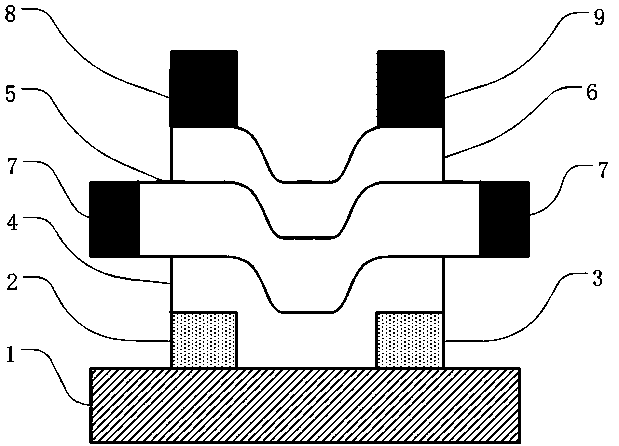
[0038] a. On the transparent substrate 1, by magnetron sputtering method, two conductive electrodes with high work function, the hole transport layer source 2 and the hole transport layer drain 3, are deposited;

[0039] b. On the two electrodes and the transparent substrate 1, a hole transport layer 4 is formed by vacuum evaporation or spin coating;

[0040] c. On the hole transport layer 4, grow a light emitting layer 5 by vacuum evaporation or spin coating;

[0041] d. On the growing luminescent layer 5, grow the electron transport layer 6 by vacuum evaporation or spin coating;

[0042] e. On the electron transport layer 6, grow an electron transport layer drain 8 and an electron transport layer source 9 with a lower work function by vacuum evaporation, and grow a lower work function on both sides of the light emittin...

Embodiment 1

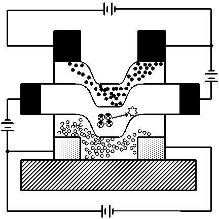
[0044] A transparent glass substrate is selected, and two ITO hole transport layer source electrodes and hole transport layer drain electrodes are grown by magnetron sputtering. N, N-bis-(naphthyl)-N, N'-diphenyl-1, 1 The hole transport layer made of '-biphenyl-4, 4'-diamine (NPB) was replaced by vacuum evaporation on a 3 cm wide × 2.5 cm long mask, and 4,4'-bis (9-carbazolyl)biphenyl (CBP) as host doped with Ir(ppy) 3 [fac-tris(2-phenylpyridine)iridium]is the light-emitting layer co-evaporated and doped with 10% of the guest, and was replaced with a 2 cm wide×2.5 cm long mask to grow with 1,3,5-tris(2-N- The electron transport layer of the material of phenylbenzimidazolyl) benzene (TPBi), replaces the mask plate again, grows four aluminum electrodes by the method of vacuum evaporation and is divided into as the light-emitting layer 5 both sides of growth light-emitting layer draw-out electrode 7, the electron transport layer drain electrode 8 and electron transport layer so...

Embodiment 2

[0051] A transparent glass substrate is selected, and two ITO hole transport layer source electrodes and hole transport layer drain electrodes are grown by magnetron sputtering. N, N-bis-(naphthyl)-N, N'-diphenyl-1, 1 '-biphenyl-4, 4'-diamine (NPB) is used as the hole transport layer of the material, and the reticle is replaced by the method of vacuum evaporation on the reticle with a width of 3 cm and a length of 2.5 cm, and Alq 3 Emitting layer doped with DCJTB [4-(dicyanomethyene)-2-t-butyl-6(1,1,7,7-tetramethyljulolidyl-9-enyl)-4H-pyran] as host and 2% co-evaporated as guest , replace it with a 2 cm wide × 2.5 cm long mask to grow an electron transport layer made of Bphen (4,7-diphenyl-1,10-phenanthroline), replace the mask again, and grow by vacuum evaporation The four aluminum electrodes are divided into lead-out electrodes 7 for growing the light-emitting layer on both sides of the light-emitting layer 5 , drain electrodes 8 of the electron-transport layer and source e...


PUM


Abstract

The invention provides an organic electroluminescent and laser luminescent device based on double TFT modulation and a manufacturing method of the organic electroluminescent and laser luminescent device. The luminescent device comprises a transparent substrate, a hole transport layer source electrode, a hole transfer layer drain electrode, a hole transfer layer, a luminescent layer extraction electrode, a luminescent layer, an electronic transfer layer, an electronic transfer layer source electrode and an electronic transfer layer drain electrode. The hole transfer layer, the luminescent layer and the electronic transfer layer are sequentially grown on the glass substrate through a high vacuum evaporation method or a spin coating method, and eventually the low work function source electrode and the low work function drain electrode are evaporated through a vacuum evaporation method, wherein the glass substrate is plated with the high work function source electrode, the high work function drain electrode and the luminescent layer extraction electrode. According to the organic electroluminescent and laser luminescent device, electron concentration and hole concentration are balanced, and exciton quenching caused by excess carriers is restrained.

Description

technical field [0001] The invention relates to the fields of microelectronics and material science, in particular to an organic electroluminescent and laser light-emitting device based on double TFT modulation and a preparation method thereof. Background technique [0002] At present, the organic electroluminescent device based on the "sandwich" structure is driven by the external voltage, and the electrons injected by the cathode and the holes injected by the anode migrate from the electron transport layer and the hole transport layer to the organic light-emitting layer respectively. Recombination in the layer releases energy, so that the organic light-emitting substance molecules are excited and transition to the excited state, and the excited molecules emit light when they return to the ground state from the excited state. [0003] In the traditional device structure, due to different organic electronic materials and hole materials, the difficulty of injecting holes and ...

Claims


Application Information

Patent Timeline
Patent Type & Authority Applications(China)
IPC IPC(8): H01L51/50H01L51/56H01S5/30
CPCH10K71/10H10K50/11H10K50/30
Inventor 张琪李明魏梦杰徐韬魏斌
Owner 浩物电子科技(苏州)有限公司
Why Eureka
Try Eureka