SMD IC welding and fixing device

A fixing device and patch technology, which is applied in the direction of auxiliary devices, welding equipment, auxiliary welding equipment, etc., can solve problems such as difficult positioning, and achieve the effects of avoiding electrical characteristics, ensuring good product rate, and reducing hard contact

Active Publication Date: 2014-03-19
JIANGSU SHENGLI DETECTION INSTR CO LTD
View PDF8 Cites 2 Cited by
  • Summary
  • Abstract
  • Description
  • Claims
  • Application Information

AI Technical Summary

Problems solved by technology

[0004] The technical problem to be solved by the present invention is to provide a chip IC welding and fixing device, which solves the problem of difficult positioning of the chip IC by manual welding in the prior art

Method used


Image

  • SMD IC welding and fixing device

Examples


Embodiment 1

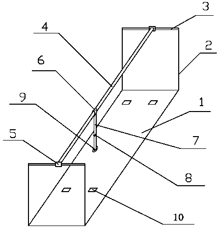
[0019] Embodiment one, such as figure 1 As shown, a patch IC welding and fixing device includes a base 1, a bracket 2, a beam 4, and a fixing member 7; The two ends of the beam 4 are respectively connected to the two brackets 2; the upper end of the fixing member 7 is connected to the beam 4 and moves along the beam 4, and the lower end is opposite to the base 1, and the fixing member 7 is used for patch IC welding Fix the IC on the pads of the PCB.

[0020] The fixing part 7 includes two parts that are connected to each other and can move relative to each other. A third connecting part 8 for making the two parts move or fix relative to each other is arranged between the two parts. The connecting piece 8 moves up and down relative to the upper end, and the third movable connecting piece 8 is provided with fastening devices such as buttons, draw-in grooves, and clips to fix the lower end. When in use, the fastening device is opened, and the third connecting piece 8 is adjusted...

Embodiment 2

[0024] Embodiment 2. A patch IC welding and fixing device, including a base 1, a bracket 2, a beam 4, and a fixing member 7; The two ends of the beam 4 are respectively connected to the two brackets 2; the upper end of the fixing member 7 is connected to the beam 4 and moves along the beam 4, and the lower end is opposite to the base 1, and the fixing member 7 is used for patch IC welding When fixing the IC on the pad of the PCB.

[0025] A second connecting piece 6 is arranged between the crossbeam 4 and the fixing piece 7, and the second connecting piece 6 is respectively movably connected with the crossbeam 4 and the fixing piece 7, and the second connecting piece 6 drives the fixing piece 7 to move along the crossbeam 4 , the fixing part 7 can move up and down relative to the second connecting part, and the second connecting part 6 is provided with a first fastener that fastens the fixing part 7 to the beam 4. When the first fastener is opened, The second connecting part ...


PUM


Abstract

The invention discloses an SMD IC welding and fixing device which comprises a base, two supports, a beam and a fixing piece. The two supports are oppositely arranged on the two ends of the base in parallel and are perpendicular to the base. The two ends of the beam are connected with the two supports respectively. The upper end of the fixing piece is connected with the beam and moves along the beam, the lower end of the fixing piece is opposite to the base, and the fixing piece is used for fixing the IC to a bonding pad of a PCB during SMD IC welding. Before welding, the SMD IC is fixed to the bonding pad of the PCB, the IC does not need to be fixed with human hands, one hand holds tin wires, the other hand holds an electric soldering iron to conduct welding, displacement cannot occur easily, welding can be achieved at a time even though an SMD IC has the very small lead pin pitch, and the yield is ensured.

Description

technical field [0001] The invention discloses a chip IC welding and fixing device, which is used for fixing the chip IC in the manual welding process in the research and development of electronic products, and belongs to the field of supporting products in the electronic industry. Background technique [0002] Electronics factories need to do various prototype debugging tests in production and R&D. In this process, manual soldering of PCB boards is unavoidable. For some conventional resistors and capacitors, skilled operators can easily complete them, but for small chip ICs, it is the most difficult. The most important thing is the process from manual alignment to soldering. After alignment, you need to fix the IC with tweezers or fingers, and you have to free your hand to hold the solder wire. The other hand needs to operate the electric soldering iron. It is difficult to align the position. Maybe Accidentally misaligned and re-aligned, and sometimes even found that the IC...

Claims


Application Information

Patent Timeline
Patent Type & Authority Applications(China)
IPC IPC(8): B23K3/08B23K37/04
CPCB23K3/087
Inventor 周桃英王香兵唐豪
Owner JIANGSU SHENGLI DETECTION INSTR CO LTD
Why Eureka
Try Eureka