
Four-station parallel testing device and method

A testing device and a four-station technology are applied to measuring devices, material analysis through optical means, instruments, etc., which can solve problems such as unfixed positions for photographing and testing, long equipment footprints, and different benchmarks, etc., to achieve Improve stability and test efficiency, reduce floor space, and reduce volume

Active Publication Date: 2014-03-26
SHENZHEN MASONE ELECTRONICS
View PDF5 Cites 10 Cited by
  • Summary
  • Abstract
  • Description
  • Claims
  • Application Information

AI Technical Summary

Problems solved by technology

like figure 1 As shown, it is a schematic diagram of the traditional PCB testing method. After the PCB board is placed on the testing device through the feeding mechanism, it is transported by the belt 10 and stopped at different stations by the sensor. For example, the PCB board is stopped by the sensor. After the test station, the upper and lower molds of the test station are pressed together to test the PCB board. After the test is completed, the tested PCB board is transferred to the next station through the belt. The disadvantage of this test method is The PCB board is transported through the belt and stopped by the friction between the PCB board and the belt. Therefore, the stopping position of the PCB board in each test is inconsistent. The position of the photo taking and testing is not fixed, and deviations are prone to occur, resulting in the critical position of the CCD. The photographing and testing stations are not on the same benchmark, resulting in a lower test yield, and because the stations of this test device are distributed in a linear manner, the equipment is long and occupies a large area, and the operating efficiency is not high

Method used


Image

  • Four-station parallel testing device and method
  • Four-station parallel testing device and method
  • Four-station parallel testing device and method

Examples


Embodiment Construction

[0025] The present invention will be further described below in conjunction with the accompanying drawings and embodiments.

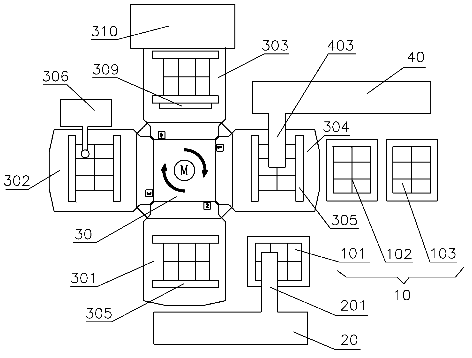
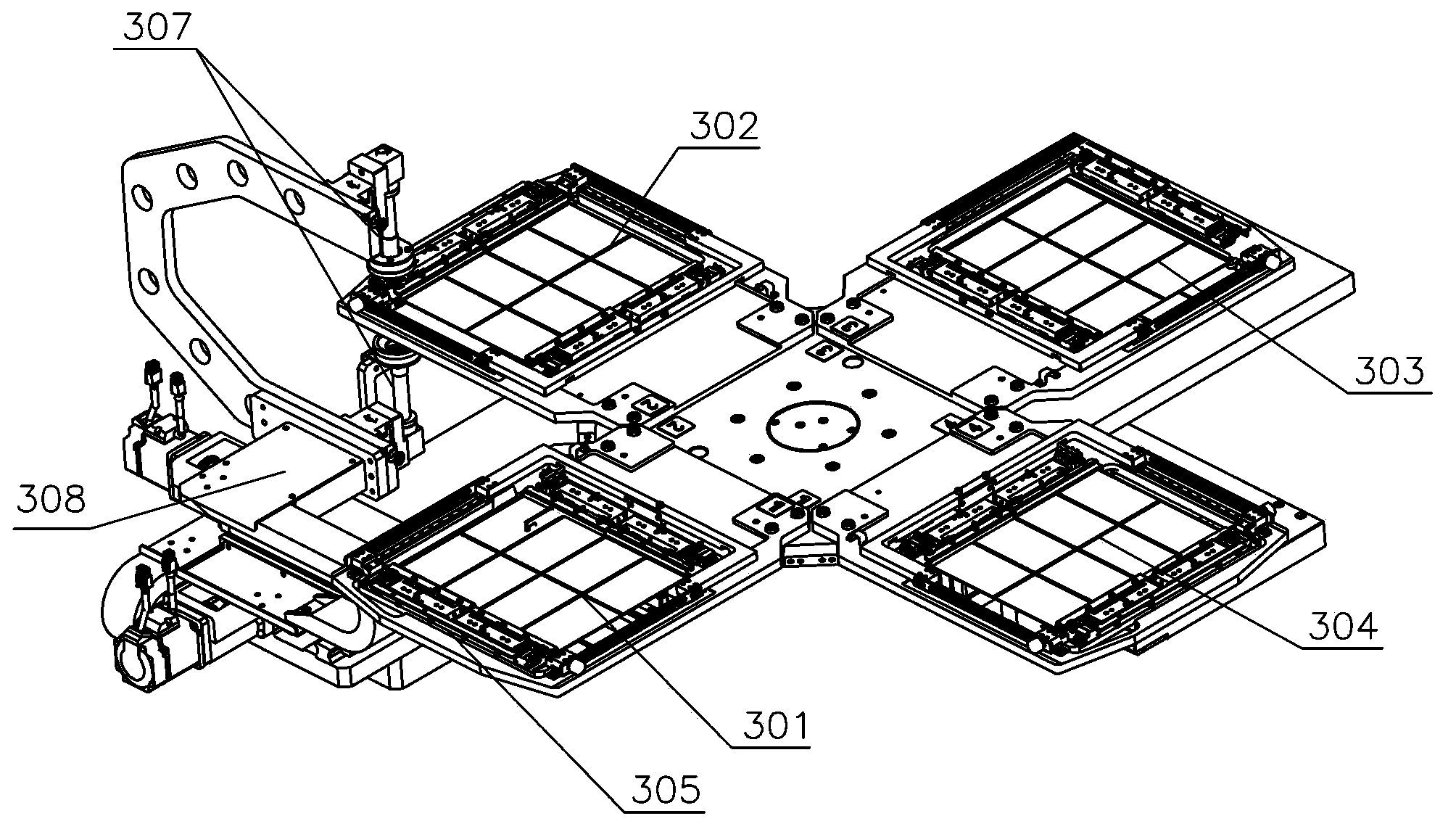
[0026] refer to figure 2 As shown, the present invention discloses a four-station parallel testing device for testing PCB boards, the testing device comprising:

[0027] A PCB material table 10, the PCB material table 10 is provided with three areas: a PCB board placement area 101 to be tested, a pass area (PASS) 102 and a failure area (FAIL) 103, which are respectively used to prevent the PCB board to be tested, Qualified PCB boards and unqualified PCB boards;

[0028] A feeding mechanism 20, which is installed next to the PCB board placement area 101 to be tested, consists of a movable water balance arm 201, a lifting cylinder located at the end of the horizontal cross arm 201, and a cylinder connected to the lifting cylinder The vacuum nozzle on the rod (the lifting cylinder and the vacuum nozzle are not marked in the figure);

[0029] A rotating...


PUM


Abstract

The invention discloses a four-station parallel testing device and a method and relates to the technical field of printed circuit board (PCB) test. The four-station parallel testing device comprises a PCB material table, a feeding mechanism, a rotary test bed, a material taking mechanism and a data processing center, wherein the data processing center is respectively connected with the feeding mechanism, the rotary test bed and the material taking mechanism and is used for controlling operations among the mechanisms. According to the rotary testing device and the method, independent operation is realized among the stations, and the testing accuracy is greatly improved. Moreover, the position of the PCB is fixed during each process, the testing stability is improved.

Description

【Technical field】 [0001] The invention relates to the technical field of PCB testing, and more specifically, the invention relates to a four-station parallel testing device and a testing method thereof. 【Background technique】 [0002] With the breakthrough of HDI process technology and the wide application of HDI boards, the testing process and methods for HDI boards are relatively lagging behind. The current method in the industry is that the PCB moves to the designated area through an automatic line, then takes pictures, then tests, and finally distinguishes . Such as figure 1 As shown, it is a schematic diagram of the traditional PCB testing method. After the PCB board is placed on the testing device through the feeding mechanism, it is transported by the belt 10 and stopped at different stations by the sensor. For example, the PCB board is stopped by the sensor. After the test station, the upper and lower molds of the test station are pressed together to test the PCB b...

Claims


Application Information

Patent Timeline
Patent Type & Authority Applications(China)
IPC IPC(8): G01N21/84
Inventor 王锐胡泉金杨朝辉石磊
Owner SHENZHEN MASONE ELECTRONICS
Learn More