Single event effect detecting device of image sensor

A single-event effect and image sensor technology, which is applied in the direction of measuring devices, instruments, and measuring electronics, can solve the problems of image sensor imaging function failure and single-event function interruption, and achieve convenient single-particle test process, high-speed data transmission, and convenient The effect of control

Active Publication Date: 2014-03-26
BEIJING MXTRONICS CORP +1
View PDF8 Cites 7 Cited by
  • Summary
  • Abstract
  • Description
  • Claims
  • Application Information

AI Technical Summary

Problems solved by technology

When the particle bombards the control unit, it may cause the imaging function o

Method used


Image

  • Single event effect detecting device of image sensor
  • Single event effect detecting device of image sensor
  • Single event effect detecting device of image sensor

Examples


Embodiment Construction

[0034] Below in conjunction with accompanying drawing and specific embodiment the present invention is described in further detail:

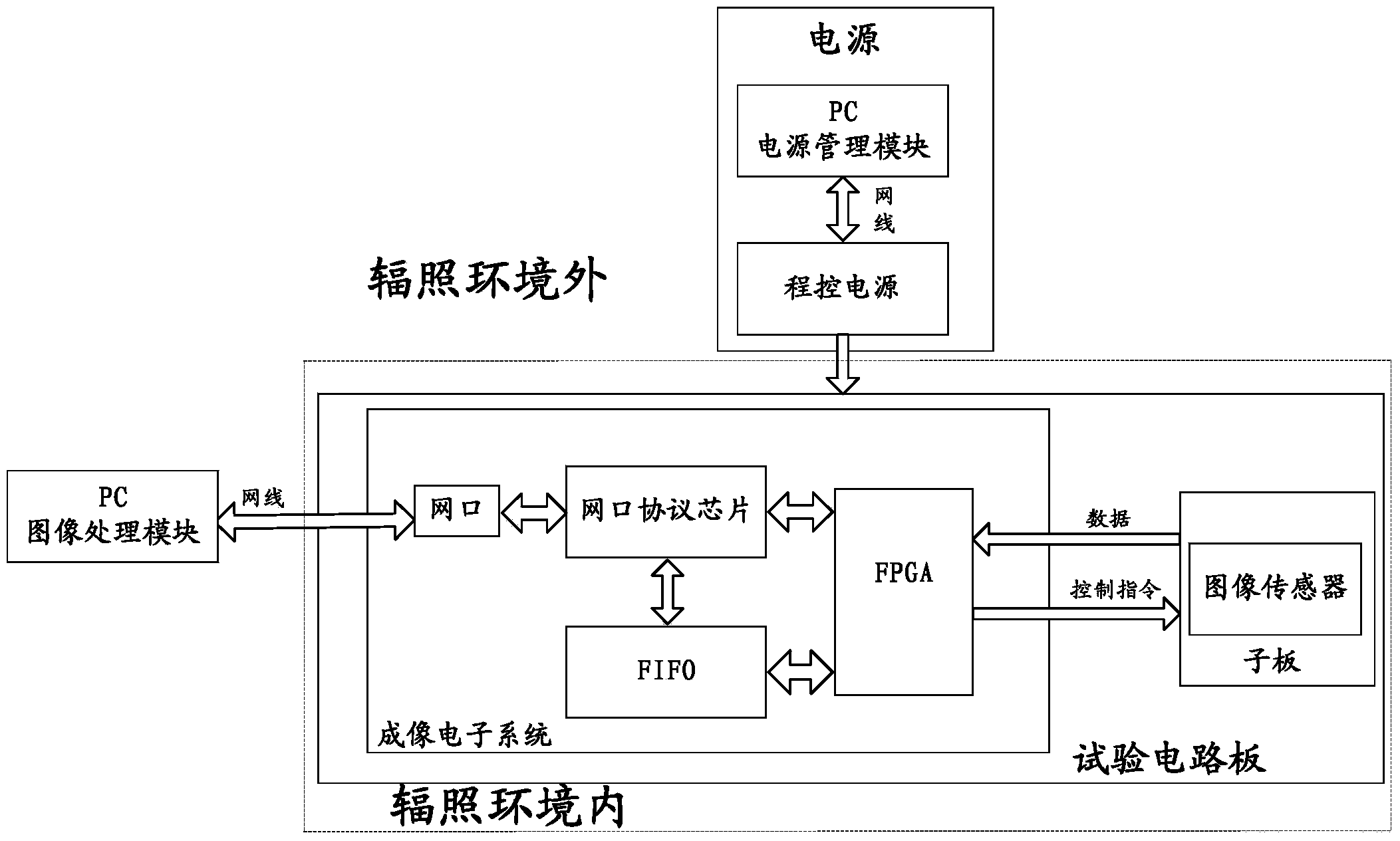
[0035] Such as figure 1 Shown is a schematic structural diagram of the single event effect detection device of the image sensor of the present invention. It can be seen from the figure that the single event effect detection device of the image sensor of the present invention includes an image processing module, a power supply and a test circuit board, and the power supply includes a power management module and a programmable power supply. The test circuit board is placed in the irradiation environment, and the image processing module and power supply are placed outside the irradiation environment. An imaging electronic system and an image sensor to be detected are arranged on the test circuit board, and the imaging electronic system includes a network port, a network port protocol chip, FIFO and FPGA.

[0036] The image processing module is res...


PUM


Abstract

The invention relates to a single event effect detecting device of an image sensor. The detecting device comprises an image processing module, a power source, a programmable power source and a test circuit board. The test circuit board is provided with an electronic imaging system and a sensor of an image to be tested. The image processing module can recognize white spots produced by bombardment of particles and count the number of the white spots and the size of occupied pixels, the transient effect on the pixels of the image sensor from single particles produced by the bombardment of the particles can be analyzed conveniently, and the single event effect sensibility of the image sensor can be effectively detected and evaluated. According to the single event effect detecting device, the single event effect produced in the particle irradiation process can be effectively and comprehensively detected, and the single event effect resisting performance index of a device can be effectively checked.

Description

technical field [0001] The invention belongs to the technical field of microelectronic device anti-single particle ability test verification, and relates to a single particle effect detection device of an image sensor. Background technique [0002] With the rapid development of semiconductor technology, the feature size and operating voltage of devices are getting smaller and smaller. Correspondingly, the critical charge is getting smaller and smaller, and the single event effect is becoming more and more obvious. In recent years, it has been found that the single event effect has a more significant impact on the working performance of the device, and its damage mode is becoming more and more complicated. If the reason for the functional interruption or functional error of the microelectronic device is not clear, it is impossible to correctly evaluate the radiation resistance of the microelectronic device. , in the later development of microelectronic devices, it is impossib...

Claims


Application Information

Patent Timeline
IPC IPC(8): G01R31/00
Inventor 陈莉明董攀陈茂鑫李想郭立业范隆岳素格郑宏超杜守刚马建华王煌伟文圣泉毕潇于春青
Owner BEIJING MXTRONICS CORP
Why Eureka
Try Eureka