Display panel and display device

A technology of display panel and protective layer, applied in instruments, semiconductor devices, optics, etc., can solve problems such as insufficient protection, and achieve the effect of improving protection and simple manufacturing process

Active Publication Date: 2014-03-26
BOE TECH GRP CO LTD +1
View PDF8 Cites 25 Cited by
  • Summary
  • Abstract
  • Description
  • Claims
  • Application Information

AI Technical Summary

Problems solved by technology

[0007] However, the above-mentioned peripheral routing area formed by connecting the gate signal line and the data signal line through the via hole respectively through the gate metal layer, and the method of protecting the metal connection line area at the peripheral routing area by using ITO coverage , due to the thickness of the protective film layer is still relatively thin, the protection is not enough, X-Line, Y-line and other problems are still relatively serious

Method used


Image

  • Display panel and display device
  • Display panel and display device
  • Display panel and display device

Examples


Embodiment Construction

[0033] The following will clearly and completely describe the technical solutions in the embodiments of the present invention in conjunction with the accompanying drawings in the embodiments of the present invention. Obviously, the described embodiments are only some of the embodiments of the present invention, not all of them. Based on the embodiments of the present invention, all other embodiments obtained by persons of ordinary skill in the art without making creative efforts belong to the protection scope of the present invention.

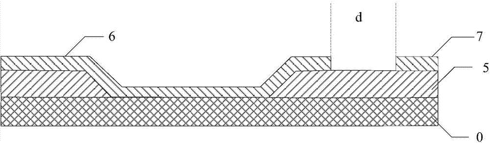
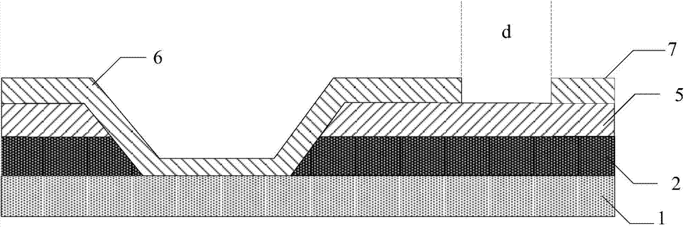
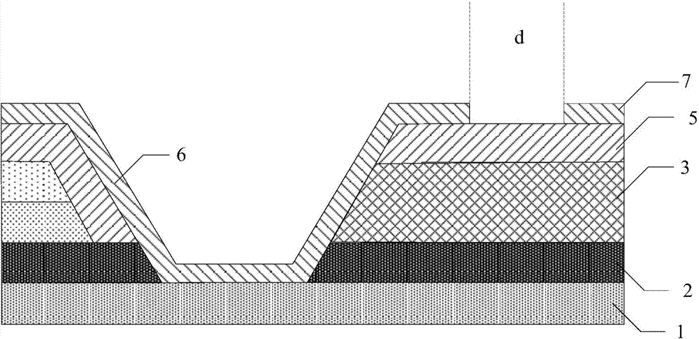
[0034] An embodiment of the present invention provides a display panel, which includes a peripheral wiring area formed by connecting the gate signal line and the data signal line respectively through via holes in the gate metal layer, such as figure 2 As shown, wherein, the metal connection line area at the peripheral wiring area includes: a gate insulating layer 2 arranged on the gate metal layer 1; and a protective layer 3 and a passivation l...


PUM


Abstract

The invention discloses a display panel and a display device in order to better protect a metal wire connecting area in the peripheral wire area, improve protection strength and prevent a wire from being broken. The display panel comprises a grid insulation layer arranged on a grid metal layer, a protective layer, a passivation layer and an ITO covering layer, wherein the protective layer, the passivation layer and the ITO covering layer are sequentially arranged on the grid insulation layer. By means of the display panel and the display device, the thickness of a film layer in the peripheral wire area can be increased, and therefore the whole peripheral wire area especially the metal connecting wire area exposed outside a color film panel can be protected, and protection strength is improved.

Description

technical field [0001] The present invention relates to the field of display technology, in particular to a display panel and a display device. Background technique [0002] With the continuous development of display technology, thin film transistor liquid crystal display devices are more and more widely used. [0003] The display panel of the existing thin film transistor liquid crystal display device has a peripheral wiring area formed by passing the signal line inside the display panel through the via hole transfer technology, including the peripheral wiring area on the signal line side and the peripheral wiring area on the gate line side, wherein, The peripheral routing area on the signal line side is made of the data metal layer (SD metal layer) that makes the source electrode and drain electrode of the thin film transistor. The gate metal layer leads out the gate signal line. [0004] In the production process, in the peripheral wiring area, it is necessary to lead o...

Claims


Application Information

Patent Timeline
Patent Type & Authority Applications(China)
IPC IPC(8): G02F1/1362G02F1/1368G02F1/13
CPCG02F1/133345G02F1/1345H01L27/124H01L29/78606G02F1/133388G02F1/136227G02F1/136286G02F1/1368
Inventor 张明王满满张国强樊超王其辉白忠飞
Owner BOE TECH GRP CO LTD
Why Eureka
Try Eureka