Semiconductor device and manufacturing method thereof

A manufacturing method and semiconductor technology, applied in semiconductor/solid-state device manufacturing, semiconductor devices, electric solid-state devices, etc., can solve problems such as limited performance improvement, small process window, and limited product yield, so as to improve performance and reduce The effect of loss

Active Publication Date: 2017-05-10
SEMICON MFG INT (BEIJING) CORP +1
View PDF3 Cites 13 Cited by
  • Summary
  • Abstract
  • Description
  • Claims
  • Application Information

AI Technical Summary

Problems solved by technology

[0004] However, the performance improvement of PMOS devices formed by the existing technology is limited, the process window is small, and the product yield is limited

Method used


Image

  • Semiconductor device and manufacturing method thereof
  • Semiconductor device and manufacturing method thereof
  • Semiconductor device and manufacturing method thereof

Examples


Embodiment Construction

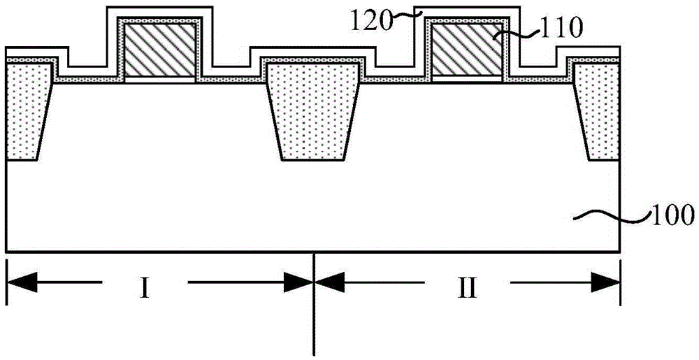
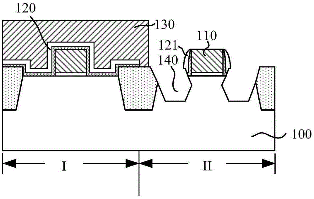
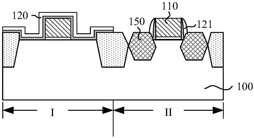
[0030] refer to Figure 1 to Figure 4 , in the prior art semiconductor manufacturing process, the formation process of the semiconductor device includes the following steps:

[0031] A semiconductor substrate 100 (such as figure 1 shown), a gate structure 110 (such as figure 1 shown), a layer of dielectric layer 120 is conformally covered on the semiconductor substrate 100 and the gate structure 110 (such as figure 1 shown); on the semiconductor substrate 100, a patterned first mask layer 130 (such as figure 2 As shown), the patterned mask layer 130 covers the NMOS region I, using the patterned mask layer 130 as a mask, through an etching process on both sides of the PMOS region II gate structure 110 A trench 140 is formed in the semiconductor substrate 100 (such as figure 2 As shown), a side wall 121 is formed on the side wall surface of the gate structure 110 of the PMOS region II, and the shape of the trench 140 is a Sigma shape; a stress layer 150 is filled in the ...


PUM


Abstract

The invention provides a semiconductor device and manufacturing method thereof. The method includes providing a semiconductor substrate; forming a gate structure on the semiconductor substrate; forming epitaxial substrate layers on the semiconductor substrate at both sides of the gate structure; forming hard mask side wall layers on side walls of the gate structure; using the hard mask side wall layers as masks, etching the epitaxial substrate layers and the semiconductor substrate, and forming trenches at both sides of the gate structure; and forming stress layers in the trenches. According to the method provided by the invention, the epitaxial substrate layers serve as a part of a PMOS device substrate, so that the PMOS device substrate is lifted and the lifted height of the substrate can be controlled through adjustment of the thickness of the epitaxial substrate layers, thereby ensuring that loss of an oxidation layer close to the bottom of the gate by an etching process for forming the trenches is reduced while pressure stress is applied to a PMOS channel region to improve the hole mobility, thereby avoiding the problem of a short circuit between the gate structure and source and drain regions, and improving the performance of a semiconductor device.

Description

technical field [0001] The invention relates to the field of semiconductors, in particular to a semiconductor device and a manufacturing method thereof. Background technique [0002] In semiconductor manufacturing, with the development trend of ultra-large-scale integrated circuits, the feature size of integrated circuits continues to decrease, the size of transistors is getting smaller and smaller, and the operating speed is getting faster and faster. Therefore, the requirements of semiconductor manufacturing processes for transistor performance are also increasing. Higher and higher. Carrier mobility is one of the main factors affecting the performance of transistors, and effectively improving carrier mobility has become one of the key points in the manufacturing process of transistor devices. [0003] In the manufacturing technology of complementary metal-oxide-semiconductor field-effect transistor (CMOS) devices, it is common to treat P-type metal-oxide-semiconductor fi...

Claims


Application Information

Patent Timeline
Patent Type & Authority Applications(China)
IPC IPC(8): H01L27/092H01L21/8238
CPCH01L21/8238H01L27/092H01L29/66628H01L29/66636H01L29/0847H01L29/165H01L29/7848H01L21/02532H01L21/02529H01L21/02546H01L21/0262H01L21/3065H01L21/3081H01L21/3085H01L21/3086H01L29/161H01L21/31116H01L21/30608H01L29/0653H01L27/0924H01L21/823821H01L21/823814
Inventor 徐长春
Owner SEMICON MFG INT (BEIJING) CORP
Why Eureka
Try Eureka