Low-power-consumption on-chip network task mapping method

An on-chip network and task mapping technology, applied in special data processing applications, instruments, electrical digital data processing, etc., can solve problems such as increased energy consumption and time-consuming, and achieve the effect of reducing mapping power consumption and improving mapping efficiency

Active Publication Date: 2014-03-26
湖州信倍连网络科技有限公司
View PDF2 Cites 3 Cited by
  • Summary
  • Abstract
  • Description
  • Claims
  • Application Information

AI Technical Summary

Problems solved by technology

Existing mapping methods often use complex methods for mapping, and it takes a lot of time to calculate the mapping process, which also increases energy consumption to some extent

Method used


Image

  • Low-power-consumption on-chip network task mapping method
  • Low-power-consumption on-chip network task mapping method
  • Low-power-consumption on-chip network task mapping method

Examples


Embodiment Construction

[0021] In order to make the object, technical solution and advantages of the present invention clearer, the present invention will be further described in detail below in conjunction with the accompanying drawings and embodiments. It should be understood that the specific embodiments described here are only used to explain the present invention, not to limit the present invention.

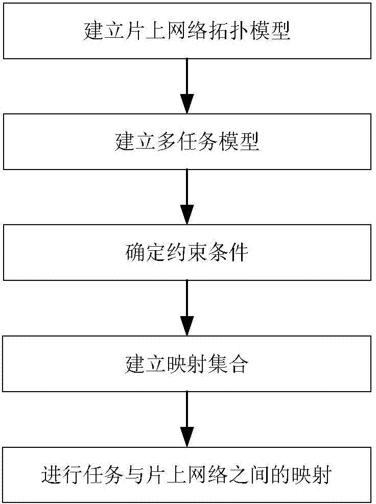
[0022] Such as figure 1 As shown, a low-power on-chip network task mapping method of the present invention includes the following steps:

[0023] S10: Establish an on-chip network topology model

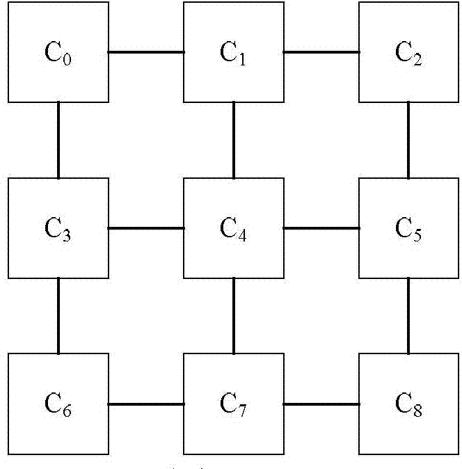
[0024] For the network on chip, it is represented by N(C, P), where C is the processor core C n The set of , P is the path P ij set; among them, P ij Indicates slave processor core C i to the processor core C j of a path. while s=|C i →C j |Indicates the slave processor core C i to the processor core C j The number of on-chip network routers passed; E bit Indicates the average energy consumpti...


PUM


Abstract

The invention discloses a low-power-consumption on-chip network task mapping method. The low-power-consumption on-chip network task mapping method comprises the following steps of S10, building an on-chip network topology model, S11, building a multi-task model, S12, determining constraint conditions, S13, setting up a mapping set, and S14, carrying out mapping between tasks and an on-chip network. According to the low-power-consumption on-chip network task mapping method, due to the facts that the model is built for the tasks in the on-chip network, the relation among the tasks is analyzed, and then the tasks are mapped through dual constraint conditions including communication delay and energy consumption, mapping efficiency is improved, and power consumption of mapping is reduced.

Description

technical field [0001] The invention belongs to the field of on-chip network technology, and relates to a low-power on-chip network task mapping method. Background technique [0002] As the main frequency of general-purpose processors breaks through 4GHz, people find that simply increasing the main frequency can no longer effectively improve performance, but instead brings about a sharp increase in power consumption, and the road to high frequency has gradually come to an end. So the research on computer processors began to turn to the direction of multi-processing cores. Early symmetric multiprocessors (SMP) mostly used the method of bringing together a group of CPUs on the same computer, and shared memory subsystems and bus structures among them. Later, due to the introduction of nanoscale manufacturing processes, SMP began to transform into a single-chip multiprocessor (Chip Multiprocessor, CMP), that is, multiple processing cores are integrated on the same chip, forming...

Claims


Application Information

Patent Timeline
Patent Type & Authority Applications(China)
IPC IPC(8): G06F15/163G06F17/50
Inventor 胡威邹代坤郭宏黎文飞张凯江若成李伟强谭练张若凡徐景
Owner 湖州信倍连网络科技有限公司
Why Eureka
Try Eureka