Serial thermal linear processor arrangement

A thermal processor and processor technology, applied in semiconductor/solid-state device manufacturing, electrical components, circuits, etc., can solve the problems of difficult cleaning and high cost of processing equipment, achieve uniform and controllable heating, improve system requirements, and transmit Simple and controllable effect of mechanical system

Active Publication Date: 2014-03-26
PSK INC +1
View PDF18 Cites 4 Cited by
  • Summary
  • Abstract
  • Description
  • Claims
  • Application Information

AI Technical Summary

Problems solved by technology

Due to the nature of the fluxes used in the prior art, these fluxes tend to adhere to the handling equipment, making it dif

Method used


Image

  • Serial thermal linear processor arrangement
  • Serial thermal linear processor arrangement
  • Serial thermal linear processor arrangement

Examples


Embodiment Construction

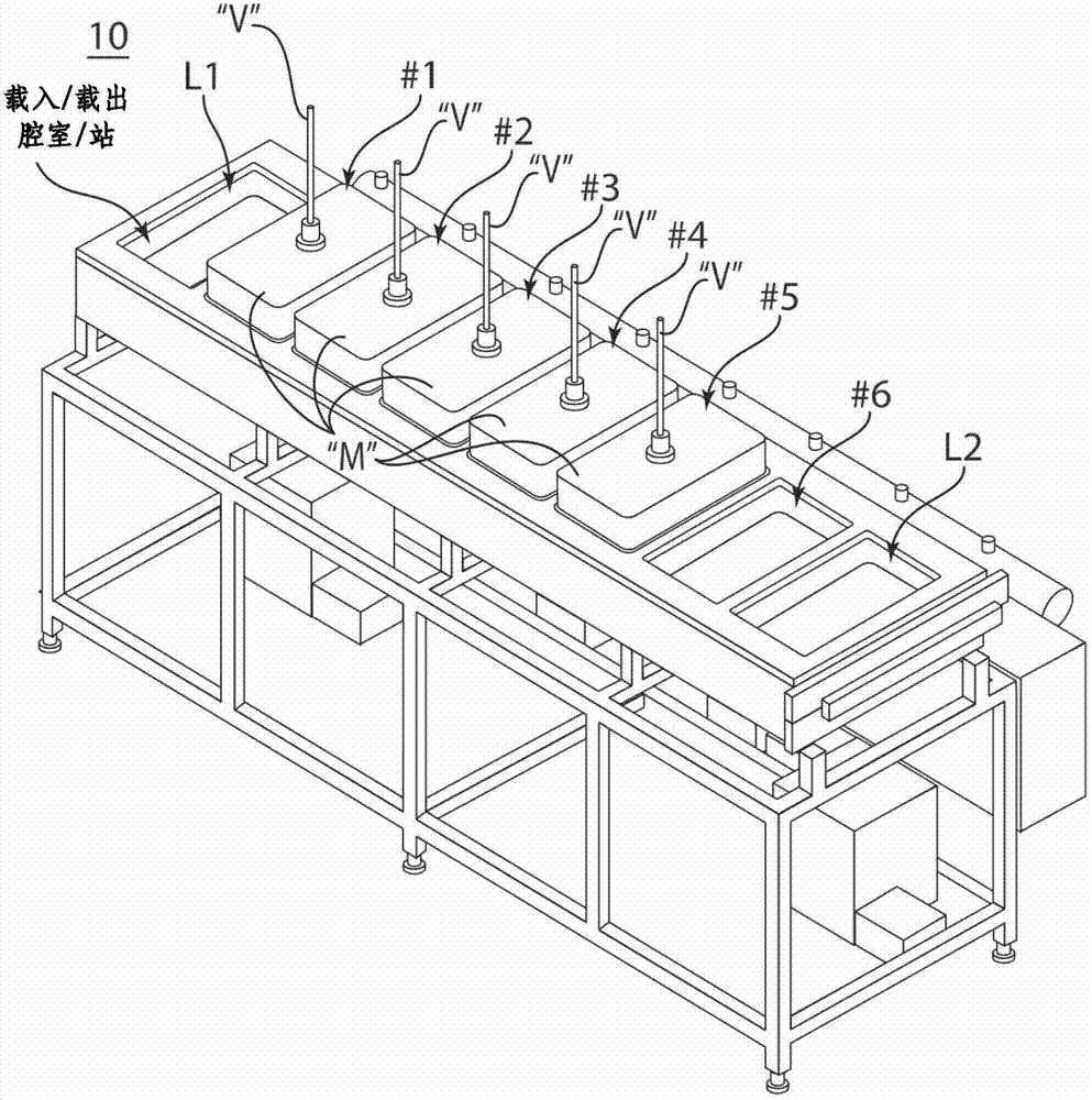
[0046] The present invention encompasses electronic chips fabricated by a stepwise and linear series of thermal processor arrays 10, wherein the fabrication method is a series of thermal processor arrays 10 sequentially passing through a series of at least six separate and enclosed chambers / station, the initial loading / unloading chamber / station and the final loading / unloading chamber / station processing the chip / substrate assembly W prior to processing, as above figure 1 shown.

[0047] Such as figure 1 The serial linear thermal processor array 10 shown is arranged to progressively process material, for example, a semiconductor substrate assembly, in a series of linearly arranged and spatially separated locations, starting with an initial load / unload chamber / station to each numbered processing chamber / station, for example: the first, second, third, fourth, fifth and sixth chamber / station, wherein the temperature, pressure and presence of each chamber / station The gases can b...


PUM


Abstract

A linear, serial chip/substrate assembly processing machine for stepwise advancing a pre-assembled chip/die substrate on a support plate through a series of sealable chambers having displacable bottom processing portions. The process begins at a loading station and ends up at an unloading station after various melting and vacuuming of chip/substrate components supported on a device tray through those various chambers to the final joining thereof.

Description

technical field [0001] The present invention relates to electronic chips and methods of manufacturing such electronic chips, such as semiconductor substrates, and more particularly, the present invention relates to step-by-step processes for equipment for the manufacture of semiconductor substrates, and is related to U.S. Patent Application (US8,274,161 , announced on September 25, 2012) is a partial continuation of divisional applications with similar technical features. This US patent application (US8,274,161) is another US patent application (No.12 / 930203, filed on December 2010 Partial continuous application until March 31). This application claims priority to the U.S. patent application (No. 12 / 930203), and is also part of the continuation application of the U.S. patent application (No. 12 / 653,454, filed on December 14, 2009), which is another Divisional application of US patent application (No.11 / 482,838, filed on July 07, 2006, current patent number is US7,008,879). T...

Claims


Application Information

Patent Timeline
IPC IPC(8): H01L21/48
CPCH01L21/4825H01L21/67173
Inventor 张健
Owner PSK INC
Why Eureka
Try Eureka