Pressure sensor array and its preparation method
A pressure sensor and array technology, applied in the sensor field, can solve the problems of sensitivity and low resolution of the pressure sensor, and achieve the effects of saving preparation cost, simple preparation process and simple structure
- Summary
- Abstract
- Description
- Claims
- Application Information
AI Technical Summary
Problems solved by technology
Method used
Image
Examples
Embodiment 1
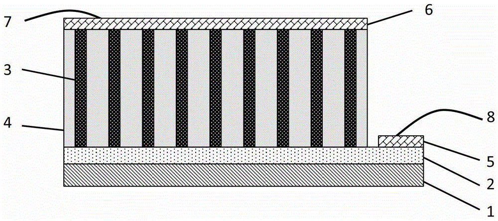
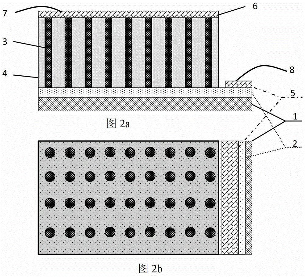
[0037] For the pressure sensor array in this embodiment, see figure 1 and Fig. 2, including: substrate 1; semiconductor film layer 2 on the substrate; nanowires or nanorod arrays 3 with piezoelectric properties on the semiconductor film layer 2; gaps between nanowires or nanorod arrays 3 are filled with dielectric Material 4, the dielectric material may be transparent or non-transparent or translucent; an upper electrode 6 on the nanowire or nanorod array 3; and a lower electrode 5 on the semiconductor thin film layer 2. Wherein, the nanowire or nanorod array 3 forms a luminescent PN junction with the semiconductor thin film layer 2 . The pressure sensor array also includes upper electrode lead-out wires 7 and lower electrode lead-out wires 8 that are necessarily related to the pressure sensor array according to the present invention, and are used to apply a driving voltage to the pressure sensor array device.
[0038] Since the nanowire or nanorod array 3 forms a light-emitt...
Embodiment 2
[0068] For the pressure sensor array in this embodiment, see Figure 4 , fabricated on the substrate 11, including: the bottom electrode 21 on the substrate 11, the sensing cell array on the bottom electrode 21 and the top electrode 61 on the sensing cell array, wherein the sensing cell is composed of the region 31 and the region 41 to form a light-emitting PN junction, wherein the material of the P-type region and / or N-type region of the PN junction is a piezoelectric material; the gap of the sensing unit is filled with a dielectric material 51, and the dielectric material 51 can be Transparent or opaque or translucent. The pressure sensor array also includes wires 71 and wires 81 drawn from the bottom electrode 21 and the top electrode 61 , which are necessarily related to the pressure sensor array according to the present invention. In the present invention, light-emitting diodes (PN junctions) are used as basic pixel units, and driving voltages are applied to the wires 71...
PUM
 Abstract
Description
Claims
Application Information


