Thin film forming method and thin film forming apparatus
A technology of thin film and thin film material, applied in the field of thin film formation and thin film forming device
- Summary
- Abstract
- Description
- Claims
- Application Information
AI Technical Summary
Problems solved by technology
Method used
Image

Examples
Embodiment 1
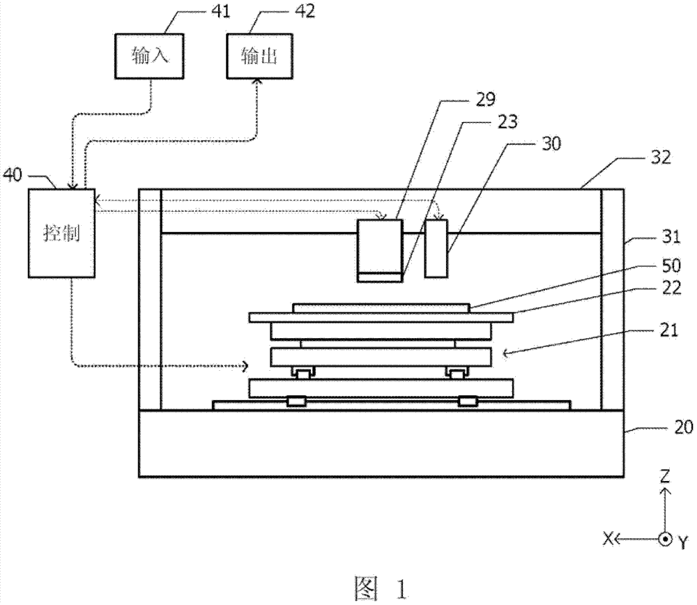
[0067] figure 1 A schematic view of the thin film forming apparatus of Example 1 is shown in . A stage 22 is supported on the platform 20 via a moving mechanism 21 . A substrate 50 such as a printed wiring board is held on the upper surface (holding surface) of the stage 22 . An XYZ rectangular coordinate system is defined by setting the directions parallel to the holding surface of the stage 22 as the X direction and the Y direction, and taking the normal direction of the holding surface as the Z direction. The moving mechanism 21 moves the stage 22 in the X direction and the Y direction.
[0068] The beam 32 is supported above the platform 20 via the struts 31 . The nozzle unit support mechanism 29 and the imaging device 30 are attached to the beam 32 . The nozzle unit 23 is supported on the nozzle unit support mechanism 29 . The imaging device 30 and the nozzle unit 23 face the substrate 50 held on the stage 22 . The imaging device 30 images a wiring pattern formed on...
Embodiment 2
[0098] Next, the thin film forming method of Example 2 will be described with reference to FIGS. 7A to 7E . Hereinafter, differences from Embodiment 1 will be described, and descriptions of the same configuration will be omitted. The edge pattern 60 shown in FIG. 4A of the first embodiment is formed by the first scanning.
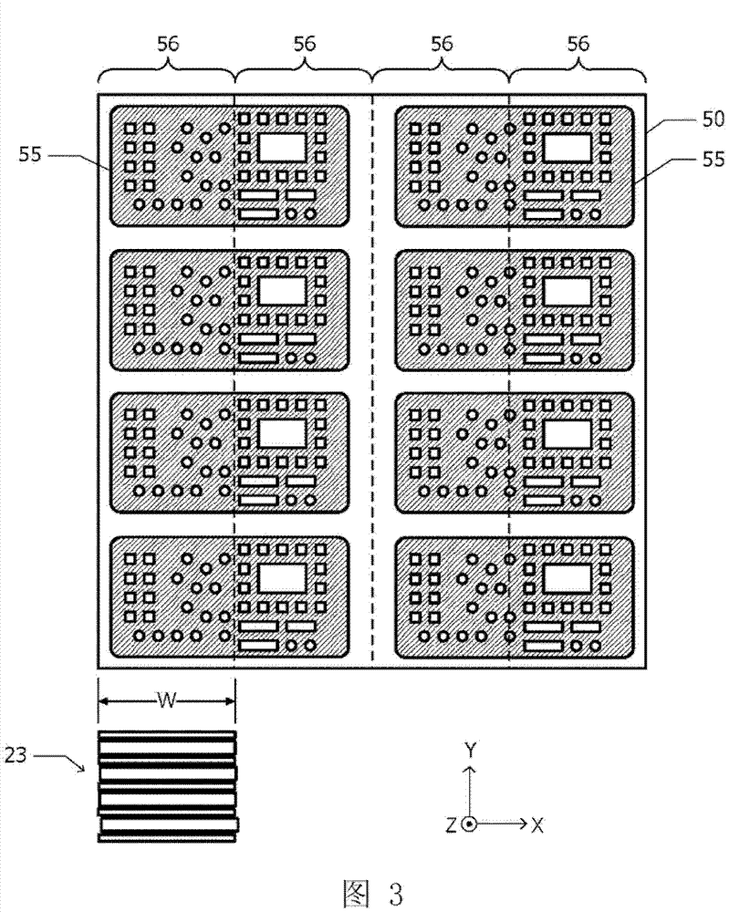
[0099] FIG. 7A shows a plan view of the substrate 50 and the nozzle unit 23 before and after the second scan. After the first scan, the second scan is performed by moving the substrate 50 in the positive direction of the Y axis. In the second scan, in the unit scanning area 56 ( image 3 ) in the same unit scanning area 56, an uncured planar pattern 64 is formed.
[0100] FIG. 7B shows a plan view of the substrate 50 and the nozzle unit 23 before and after the third scan. After the second scan, the third scan is performed by moving the substrate 50 in the negative direction of the Y axis without shifting in the X direction. In the 3rd scan, do not spit...
Embodiment 3
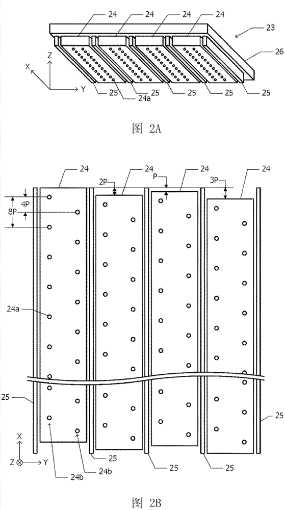
[0106] Referring to FIGS. 8A to 8D , the thin film forming method of Example 3 will be described. Hereinafter, differences from Embodiment 2 will be described, and descriptions of the same configuration will be omitted. The nozzle unit 23 ( figure 2 A) includes 4 nozzle heads 24 . The nozzle unit 23 of the thin film forming apparatus used in Example 3 includes eight nozzle heads 24 .
[0107] FIG. 8A shows a plan view of the substrate 50 and the nozzle unit 23 before and after the first scan. The nozzle unit 23 is composed of two subunits 23A and 23B. The respective structures of the subunits 23A, 23B are the same as those of the nozzle unit 23 of Embodiment 1 ( figure 2 A) have the same structure. The subunits 23A and 23B are arranged at a predetermined interval from each other in the Y direction. The subunit 23A is arranged on the positive side of the Y axis than the subunit 23B.
[0108] The first scan is performed by moving the substrate 50 in the negative directi...
PUM
| Property | Measurement | Unit |
|---|---|---|
| Diameter | aaaaa | aaaaa |
Abstract
Description
Claims
Application Information