Display device and manufacturing method for same
A display device and display panel technology, which is applied in the direction of instruments, calculations, electrical digital data processing, etc., can solve the problems of cumbersome process and large thickness of the display device, and achieve the effects of reducing process flow, reducing cost and reducing thickness
- Summary
- Abstract
- Description
- Claims
- Application Information
AI Technical Summary
Problems solved by technology
Method used
Image
Examples
Embodiment 1
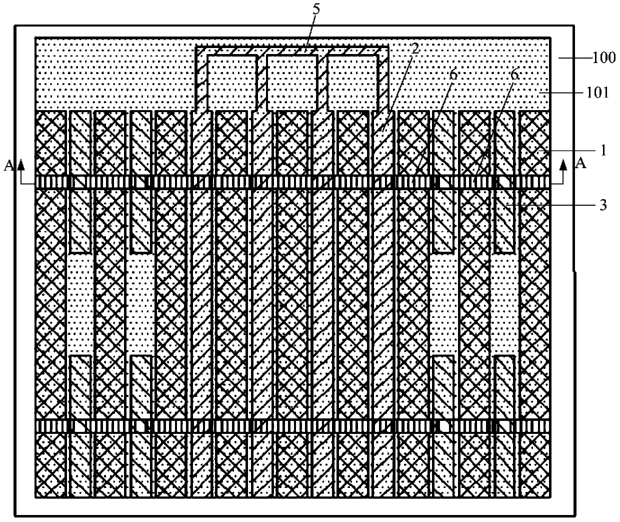
[0024] An embodiment of the present invention provides a display device integrating touch detection and 3D display, combining figure 1 , 2 As shown in and 5, the display device includes a display panel 100, a 3D grating and a touch detection unit. The display panel 100 is used to realize image display, the 3D grating is used to realize 3D display, and the touch detection unit is used to realize touch detection.
[0025] The 3D grating includes a base substrate 10 disposed on one side of the display panel 100 for displaying images. Both the grating structure and the touch sensing unit of the 3D grating are disposed between the base substrate 10 and the display panel 100 . Since a display device integrating touch detection and 3D display can be realized only by adding one base substrate 10 , the thickness of the display device is reduced, and the requirements of lightness, lightness and low cost are met. At the same time, the touch detection unit is made in the 3D grating, on...
Embodiment 2
[0041] Based on the same inventive concept, an embodiment of the present invention also provides a method for manufacturing the display device in Embodiment 1, including the steps of preparing a display panel, a 3D grating, and a touch detection unit. The display panel is used to realize picture display, the display panel is used to realize picture display, the 3D grating is used to realize 3D display, and the touch detection unit is used to realize touch detection. For image display, 3D display and touch detection, there are already very mature technologies in the prior art, which will not be described in detail here.
[0042] The 3D grating includes a base substrate, and the base substrate is arranged on one side of the display panel to display a picture. The steps of preparing the 3D grating and the touch detection unit include:
[0043] A grating structure of a 3D grating and a touch detection unit are formed between the base substrate and the display panel.
[0044] Whe...
PUM
 Abstract
Description
Claims
Application Information


