
AMOLED array basal plate and display device

An array substrate and array technology are applied in the field of AMOLED array substrates and display devices, and can solve the problems of reducing the aperture ratio of display devices and the like

Inactive Publication Date: 2014-04-02
BOE TECH GRP CO LTD
View PDF3 Cites 12 Cited by
  • Summary
  • Abstract
  • Description
  • Claims
  • Application Information

AI Technical Summary

Problems solved by technology

However, laying some cathode auxiliary lines on the non-pixel area (that is, the non-display area), specifically on the side of the gate lines, signal lines and power lines, will reduce the aperture ratio of the entire display device

Method used


Image

  • AMOLED array basal plate and display device
  • AMOLED array basal plate and display device
  • AMOLED array basal plate and display device

Examples


Embodiment Construction

[0018] The specific implementation manners of the present invention will be further described in detail below in conjunction with the accompanying drawings and embodiments. The following examples are used to illustrate the present invention, but are not intended to limit the scope of the present invention.

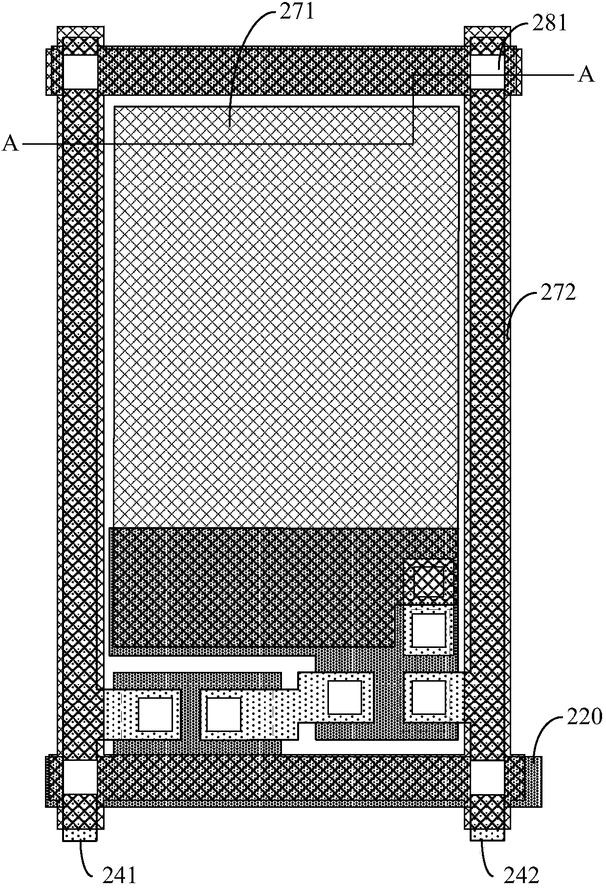
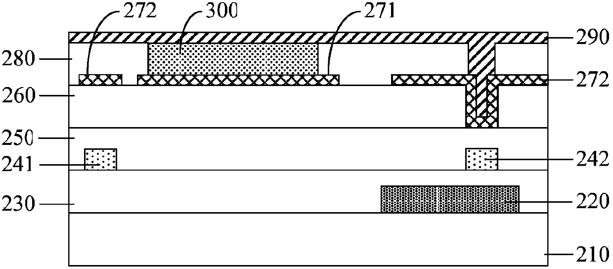
[0019] The AMOLED array substrate of the embodiment of the present invention is as figure 2 and 3 As shown, the array substrate includes several pixel structures formed in an array on the base substrate 210, and each pixel structure is surrounded by a gate line 220 and a signal line 241 and a power supply line 242 perpendicular to the gate line 220. become. Each pixel structure includes: a thin film transistor structure ( figure 2 The dotted line box in the middle), the anode 271 , the cathode 290 and the organic light-emitting layer 300 between the anode 271 and the cathode 290 . The specific hierarchy is as image 3 As shown, it includes from bottom to top: base s...


PUM


Abstract

The invention discloses an AMOLED array basal plate. The AMOLED array basal plate comprises a plurality of pixel structures formed on a substrate basal plate in an array mode; each pixel structure is formed by encircling a grid line and a signal line and a power supply line which are vertical to the grid line; each pixel structure comprises a thin film transistor structure, an anode, a cathode and an organic lighting layer between the anode and the cathode; each anode is positioned at the area corresponding to each pixel structure; each cathode is a transparent electrode covering the whole array basal plate; an insulation interval layer is formed between the anodes and the cathodes, corresponding to a non-pixel structural area; the anodes, the organic lighting layers and the cathodes form an organic light emitting diode; the grid lines, the signal lines and the power supply lines jointly drive the light emitting diode to light by the thin film transistor structures; the AMOLED array basal plate is characterized by also comprising at least one cathode auxiliary line at the same layer with the anodes and positioned at the corresponding area of the grid lines, the signal lines and the power supply lines. The cathode auxiliary line penetrates through at least two via holes of the insulation interval layer to be connected with the cathodes. Under the condition that the aperture ratio is not influenced, the cathode resistance is reduced.

Description

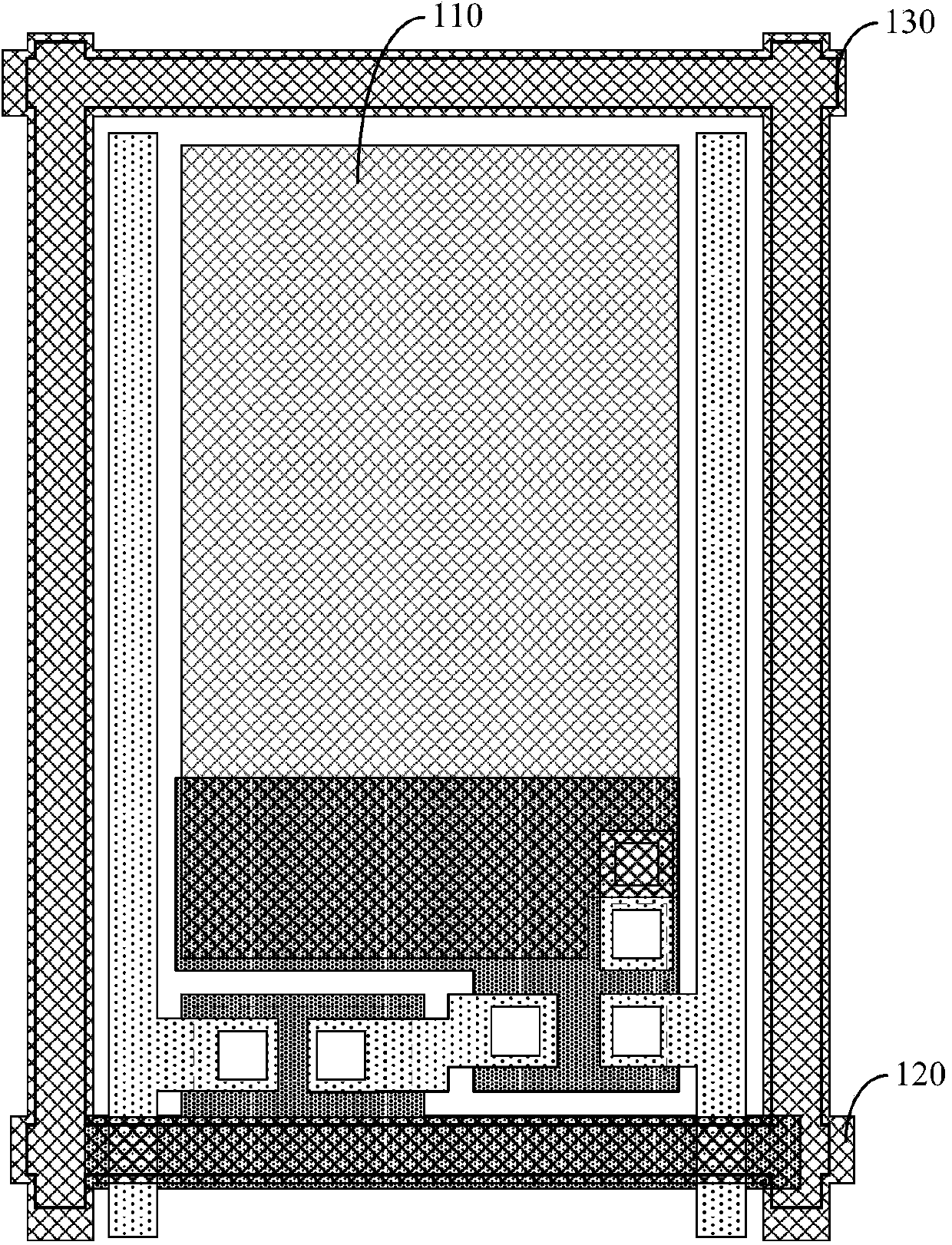
technical field [0001] The invention relates to the field of display technology, in particular to an AMOLED array substrate and a display device. Background technique [0002] For a top-emitting AMOLED display device, the cathode is formed by a transparent ITO (Indium Tin Oxide, indium tin oxide) electrode, and is a bulk electrode covering the array substrate as a whole, so the resistance of the cathode is very high. The cathode resistance is very high, which will increase the IR drop. Excessive IR drop will affect the uniformity of the picture. In order to reduce the IR drop, the existing scheme uses the cathode auxiliary line to reduce the IR drop, such as figure 1 As shown, in the non-pixel area on the array substrate, several cathode auxiliary lines are formed on different layers from the cathode, usually at the same time as the anode and / or source and drain, as shown in figure 1 The middle cathode auxiliary line 120 and the anode 110 are made of the same material and ...

Claims


Application Information

Patent Timeline
IPC IPC(8): H01L27/12H01L27/32
Inventor 永山和由
Owner BOE TECH GRP CO LTD
Learn More