Array substrate and display device

An array substrate and display area technology, which is applied to measurement devices, instruments, semiconductor devices, etc., can solve the problems of inaccurate fault location and the inability of the array substrate to be independently detected by leads, so as to achieve the effect of accurately locating the fault.

Inactive Publication Date: 2014-04-09
BOE TECH GRP CO LTD
View PDF5 Cites 17 Cited by
  • Summary
  • Abstract
  • Description
  • Claims
  • Application Information

AI Technical Summary

Problems solved by technology

[0005] The technical problems to be solved by the present invention include, aiming at the problems that the existing array substrates cannot detect each lead wire in...

Method used


Image

  • Array substrate and display device
  • Array substrate and display device
  • Array substrate and display device

Examples


Embodiment 1

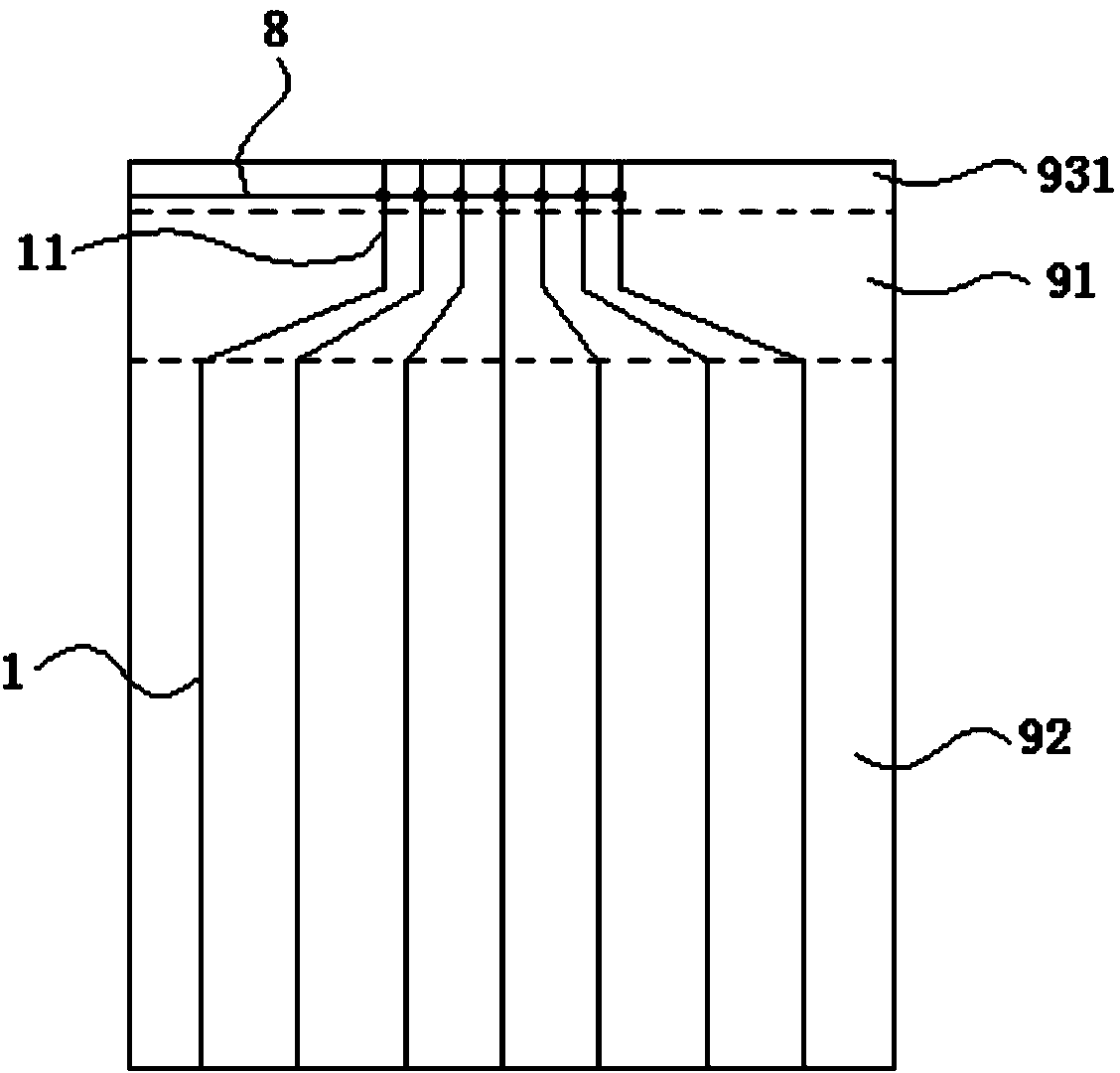
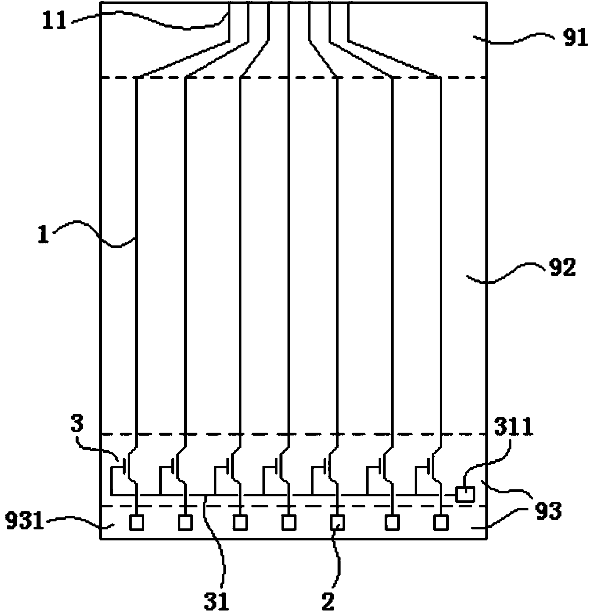
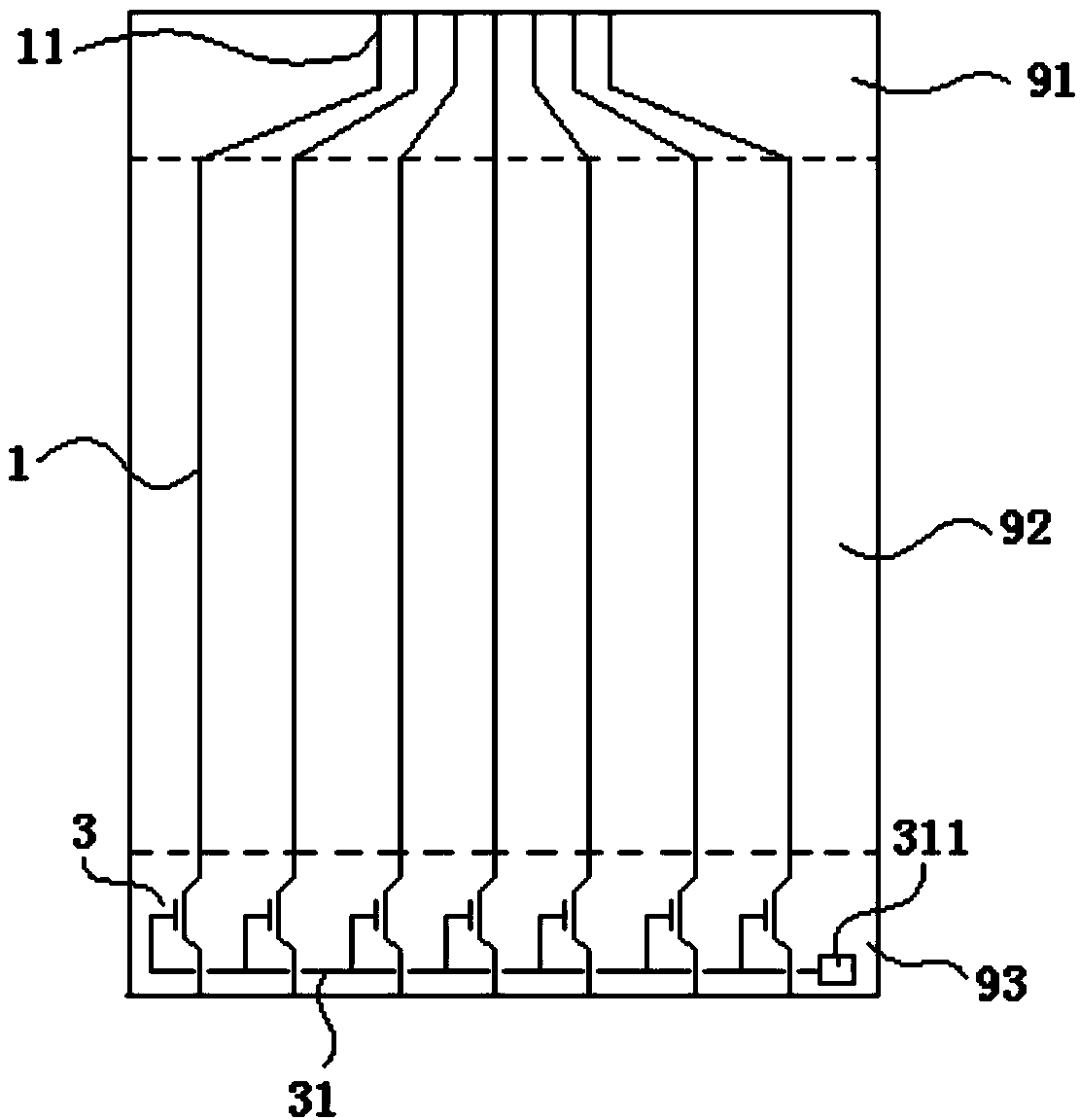
[0029] Such as Figure 2 to Figure 4 As shown, this embodiment provides an array substrate.

[0030] Preferably, the array substrate can be in different forms such as an array substrate of a liquid crystal display device, an array substrate of an organic light emitting diode display device, and the like. Depending on the type, the array substrate may have different structures such as thin film transistors, pixel electrodes, common electrode lines, cathodes, anodes, organic light-emitting layers, etc., which will not be described in detail here.

[0031] The array substrate preferably includes an expansion area 91 , a display area 92 and an edge area 93 . A plurality of lead wires 1 are arranged on the array substrate, and one end of each lead wire 1 is an input end 11 for connecting with a driving chip, and on the side of each lead wire 1 far away from the input end 11, there is also a wire for contacting with a detection probe. Connector 2.

[0032] Wherein, the display ar...

Embodiment 2

[0055] This embodiment provides a display device, which includes the above-mentioned array substrate.

[0056] The display device may be any product or component with a display function such as a liquid crystal panel, an electronic paper, an OLED panel, a mobile phone, a tablet computer, a television set, a monitor, a notebook computer, a digital photo frame, a navigator, and the like.

[0057] The display device of this embodiment includes the above-mentioned array substrate, so it can detect each data line individually, and can accurately locate the fault.


PUM


Abstract

The invention provides an array substrate and a display device, and belongs to the technical field of display. The array substrate can solve the problems that an existing array substrate cannot detect leads independently, and the fault positioning is inaccurate. The array substrate comprises an expanding area, an edge area and a display area for performing displaying, and the expanding area and the edge area are connected with the display area and located on the two non-adjacent sides of the display area respectively. A plurality of leads are arranged on the array substrate and penetrate through the display area into the edge area. One end of each lead is an input end for connecting a drive chip, and the input end of each lead is located in the expanding area. The array substrate further comprises connectors which are located on the sides, far away from the input ends, of the leads and used for detecting probe contact, and the connectors are located in the edge area.

Description

technical field [0001] The invention belongs to the field of display technology, and in particular relates to an array substrate and a display device. Background technique [0002] For a display device having a display panel such as a liquid crystal display panel, an organic light-emitting diode (OLED) display panel, etc., the display panel must first be tested before performing follow-up operations such as binding a driver IC (Driver IC), assembling, and the like. [0003] Existing detection methods for display panels such as figure 1 As shown, there is a display area 92 for displaying on the array substrate, and a large number of lead wires are arranged in the display area 92 (take the data line as an example, the gate line can be detected by a similar detection method), and one side of the display area 92 is provided with an expansion area. 91 (Fan Out), the lead wire 1 enters the display area 92 after being expanded in the development area 91, and the cutting area 931 o...

Claims


Application Information

Patent Timeline
IPC IPC(8): G02F1/13G01R31/00
CPCG02F1/1345G02F1/1362G02F1/136254H01L27/124
Inventor 金熙哲宋泳锡刘圣烈崔承镇
Owner BOE TECH GRP CO LTD
Why Eureka
Try Eureka