Cover plate structure, touch panel structure and protective panel structure of display device

A display device and touch panel technology, which is applied in the field of cover structure and protective panel structure, can solve problems such as poor bonding, easy generation of air bubbles, filling gaps, etc., and achieve the effect of reducing thickness and facilitating thinning

Inactive Publication Date: 2014-04-09
黄彩娟 +1
View PDF4 Cites 19 Cited by
  • Summary
  • Abstract
  • Description
  • Claims
  • Application Information

AI Technical Summary

Problems solved by technology

Since the ink layer 111 is also printed on the surrounding area of ​​the first substrate 110, when the first substrate 110 and the second substrate 120 are bonded together, the optical glue 116 is required to fill the central depression caused by the ink layer 111 at the same time, so that Only thicker optical glue 116 can achieve a better bonding effect, but at the same time, because optical glue 116 is a semi-solid colloid, when filling...

Method used


Image

  • Cover plate structure, touch panel structure and protective panel structure of display device
  • Cover plate structure, touch panel structure and protective panel structure of display device
  • Cover plate structure, touch panel structure and protective panel structure of display device

Examples


Embodiment 1

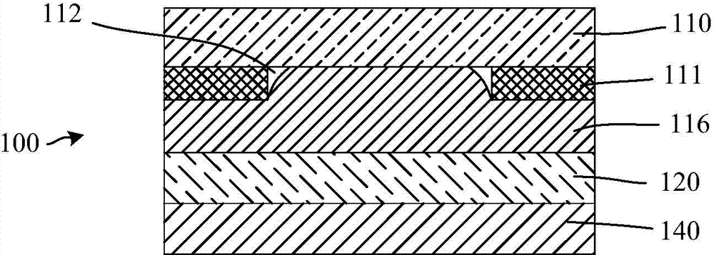
[0041] Such as figure 2 Shown is a touch panel structure 100a of a mobile phone, which includes: a first substrate 110 , a second substrate 120 and an optical adhesive 116 . Wherein, the surrounding area of ​​the first substrate 110 is printed with an ink layer 111 for forming a display area and a non-display area, and in the display area, that is, the recessed area surrounded by the ink layer on the first substrate 110 is filled with a leveling material layer 115 , used to fill the recessed area, the second substrate 120 is bonded to the display module (LCM) 140 of the mobile phone by using optical glue.

[0042] In this embodiment, the first substrate 110 adopts a glass substrate structure, and the second substrate 120 is a touch driving layer of a mobile phone. The touch driving layer may be a single-layer sensing layer structure or a double-layer sensing layer structure. The mobile phone touch panel with this structure can reduce the thickness of the optical adhesive fro...

Embodiment 2

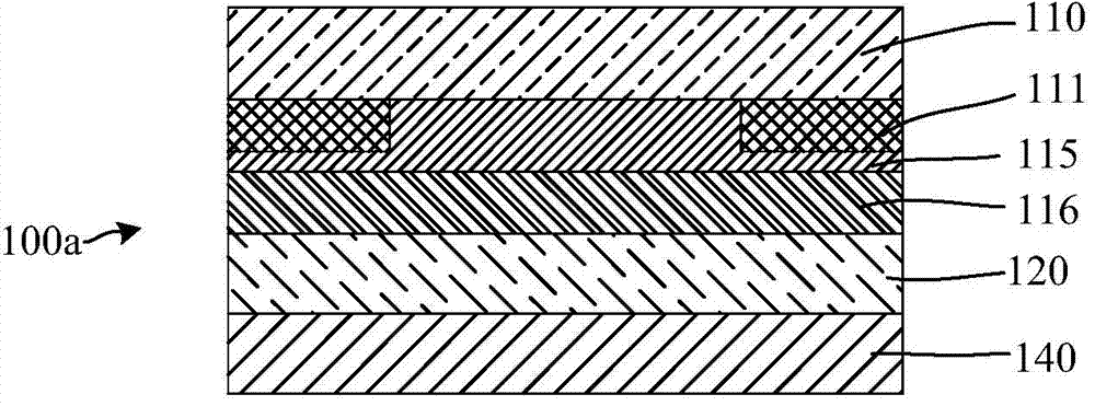
[0044] Such as image 3 Shown is another touch panel structure 100b of a mobile phone, which includes: a glass substrate 110b (first substrate), a driver module layer 120b (second substrate) and optical glue 116 . Wherein, the surrounding area of ​​the glass substrate 110b is printed with an ink layer 111, which is used to form a display area and a non-display area. In the display area, that is, the recessed area surrounded by the ink layer on the glass substrate 110b is filled with a leveling material layer 115. To fill the recessed area, the glass substrate 110b is bonded to the driver module layer 120b of the mobile phone by using optical glue.

[0045] In this embodiment, the module driving layer 120b is the combination of the touch driving layer and the display module layer of the mobile phone, that is, the touch sensing layer is directly arranged on the display module, and the ink layer 111 is printed on the glass substrate 110b After being combined with the leveling ma...

Embodiment 3

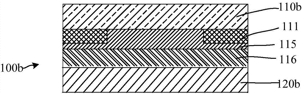
[0047] Such as Figure 4 Shown is another mobile phone touch panel structure 100c. The difference from Embodiment 1 is that the first substrate shown is a high-hardness PET substrate 110c, which plays an explosion-proof and decorative role on the surface of the mobile phone. The second substrate is a glass substrate 120c, and a capacitive sensing layer (not shown in the figure) is provided on the second substrate, namely the glass substrate 120c, to achieve touch sensing. Below the glass substrate 120c is a display module 140 (LCM) of the mobile phone . Printing or coating the ink layer 111 on the PET substrate is more advantageous than coating the ink layer 111 on the glass substrate. Because of the high hardness and material properties of the glass substrate, generally only black or white ink can be formed on the glass substrate. layer, and the processing cost is expensive, and it is also difficult to process 3D or rich colors. In this embodiment, by coating or printing th...


PUM


Abstract

The invention discloses a cover plate structure, a touch panel structure and a protective panel structure of a display device. The cover plate structure comprises a first substrate, a second substrate and optical cement for bonding the first substrate and the second substrate. An oil ink layer is printed on an area surrounding the first substrate. A filling material layer is filled in a recessed area defined by the oil ink layer on the first substrate in a display area and used for filling the recessed area. By filling the first substrate, namely the transparent substrate display area with window printing, namely the recessed area, use amount of the optical cement is less, and an optical cement layer is thin. Meanwhile, negative factors of bubbles, shadows in optical cement filling gaps and the like are avoided. By means of filling, the optical cement can achieve good bonding effect by using the thinner optical cement layer. The thickness of the whole cover plate structure can be reduced, slim design of the display device is facilitated, and integrity of the display area is facilitated.

Description

technical field [0001] The present invention relates to the field of display devices, and more specifically, to a cover structure, a touch panel structure and a protective panel structure of a display device. Background technique [0002] With the development and popularization of devices such as mobile phones, tablets, and televisions, many improvements have taken place in the structures of flat panel displays used for these devices. These improvements can continuously improve the user experience of such devices, and no matter in terms of appearance or performance, Can bring more added value to users. [0003] The upper end of the flat panel display device is generally provided with a cover structure, which mainly displays the display area by printing ink, and the display cover is also used to provide functions such as protection, decoration and touch control for the device. Such as figure 1 As shown, taking a touch cover panel of a mobile phone as an example (this displa...

Claims


Application Information

Patent Timeline
IPC IPC(8): G06F3/041
Inventor 黄彩娟潘耀铭
Owner 黄彩娟
Why Eureka
Try Eureka