Forming method of self-aligned double pattern

A dual-pattern and self-alignment technology, which is applied in electrical components, semiconductor/solid-state device manufacturing, circuits, etc., can solve problems such as poor graphics and difficult size control, and achieve stable and good device performance, consistent feature size, The effect of reducing the size of semiconductor devices

Active Publication Date: 2014-04-09
SEMICON MFG INT (SHANGHAI) CORP
View PDF5 Cites 24 Cited by
  • Summary
  • Abstract
  • Description
  • Claims
  • Application Information

AI Technical Summary

Problems solved by technology

[0009] However, in the prior art, after etching with a mask formed by a self-aligned double pat...

Method used


Image

  • Forming method of self-aligned double pattern
  • Forming method of self-aligned double pattern
  • Forming method of self-aligned double pattern

Examples


Embodiment Construction

[0034] As mentioned in the background art, in the prior art, after etching with a mask formed by a self-aligned double patterning process, the pattern formed by etching has poor morphology and is difficult to control in size.

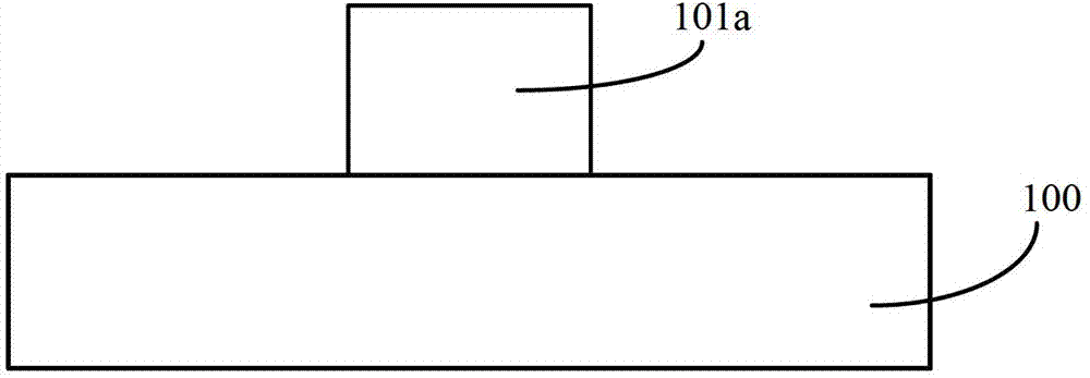
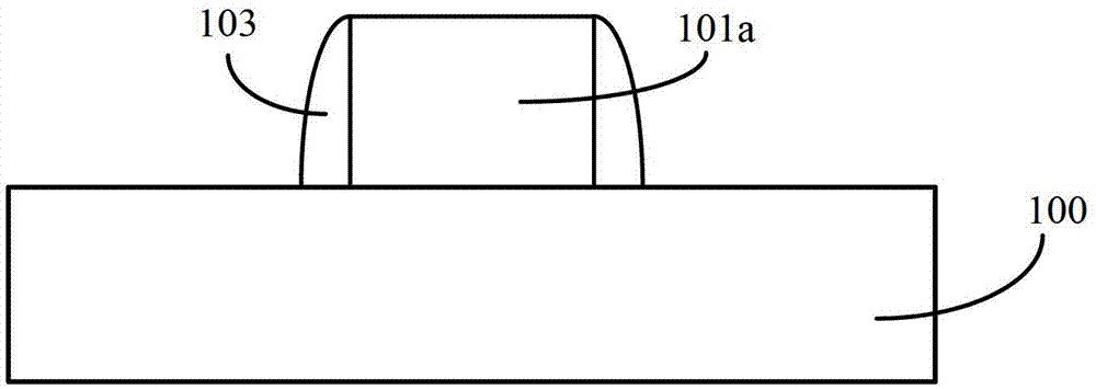
[0035] After research by the inventors of the present invention, it is found that due to the formation of the mask sidewall (such as image 3 As shown), the process is: deposit a mask layer on the surface of the semiconductor substrate 100 and the sacrificial layer 101a; etch back the mask layer until the surface of the semiconductor substrate 100 and the sacrificial layer 101a is exposed, forming a mask side wall 103; therefore, in the mask spacer 103 formed in the prior art, the sidewall of the mask spacer 103 in contact with the sacrificial layer 101a is perpendicular to the surface of the semiconductor substrate 100, and the etch-back process The other side of the formed mask spacer 103 is inclined relative to the surface of the semiconductor substr...


PUM


Abstract

The invention relates to a forming method of a self-aligned double pattern. The provided forming method comprises the following steps that: a to-be-etched layer is provided, wherein first sacrificial layers are arranged at the surface of the to-be-etched layer and the width of one first sacrificial layer is identical with the distance between the two adjacent first sacrificial layers; first mask side walls are formed at the surface of the to-be-etched layer at the two sides of the first sacrificial layers; second sacrificial layers covering the surfaces of the first mask side walls are formed at the surface of the to-be-etched layer, wherein the surfaces of the second sacrificial layers are flush with the surfaces of the first sacrificial layer; after the forming of the second sacrificial layers, the first sacrificial layers are removed and the surface of the to-be-etched layer is exposed; after removing of the first sacrificial layers, second mask side walls are formed at the second sacrificial layers and the etched layer surface at the two sides of the first mask side walls, wherein the profile shapes of the second mask side walls are symmetrical with those of the first mask side walls; and after the forming of the second mask side walls, the second sacrificial layers are removed. According to the invention, the pattern that is formed by using the formed double pattern as the mask for etching has the unified dimension and morphology.

Description

technical field [0001] The invention relates to the technical field of semiconductor manufacturing, in particular to a method for forming a self-aligned double pattern. Background technique [0002] With the continuous progress of semiconductor technology, the process nodes of semiconductor devices are continuously reduced. However, due to the limitation of the precision of the existing photolithography process, the mask pattern formed by the existing photolithography process is difficult to meet the demand for continuous reduction of the feature size of semiconductor devices, which hinders the development of semiconductor technology. [0003] In order to further reduce the size of the semiconductor device on the basis of the existing photolithography process, a double patterning process is proposed in the prior art. Among them, the self-aligned double patterning (Self-Aligned Double Patterning, SADP) process is widely used because of its simplicity. Figure 1 to Figure 5 I...

Claims


Application Information

Patent Timeline
IPC IPC(8): H01L21/308H01L21/033
CPCH01L21/0337H01L21/0338H01L21/3086H01L21/3088
Inventor 隋运奇
Owner SEMICON MFG INT (SHANGHAI) CORP
Why Eureka
Try Eureka