Substrate, alignment mark manufacturing method thereof and display device

A manufacturing method and alignment mark technology, which is applied in semiconductor/solid-state device manufacturing, electrical components, electric solid-state devices, etc., can solve problems such as reduced contrast, lower film overlap accuracy, and difficulty in identifying alignment marks

Active Publication Date: 2014-04-09
BEIJING BOE OPTOELECTRONCIS TECH CO LTD
View PDF4 Cites 1 Cited by
  • Summary
  • Abstract
  • Description
  • Claims
  • Application Information

AI Technical Summary

Problems solved by technology

However, if image 3 From the two sets of test curves A and B shown, it can be seen that the transmittance of light with a wavelength around 550nm is only 10%. The contrast of the light is reduced, which makes it difficult to identify the alignment mark and reduces the coincidence accuracy between the various films, which in turn has a negative impact on the quality of the display device

Method used


Image

  • Substrate, alignment mark manufacturing method thereof and display device
  • Substrate, alignment mark manufacturing method thereof and display device
  • Substrate, alignment mark manufacturing method thereof and display device

Examples


Embodiment Construction

[0027] The following will clearly and completely describe the technical solutions in the embodiments of the present invention with reference to the accompanying drawings in the embodiments of the present invention. Obviously, the described embodiments are only some, not all, embodiments of the present invention. Based on the embodiments of the present invention, all other embodiments obtained by persons of ordinary skill in the art without making creative efforts belong to the protection scope of the present invention.

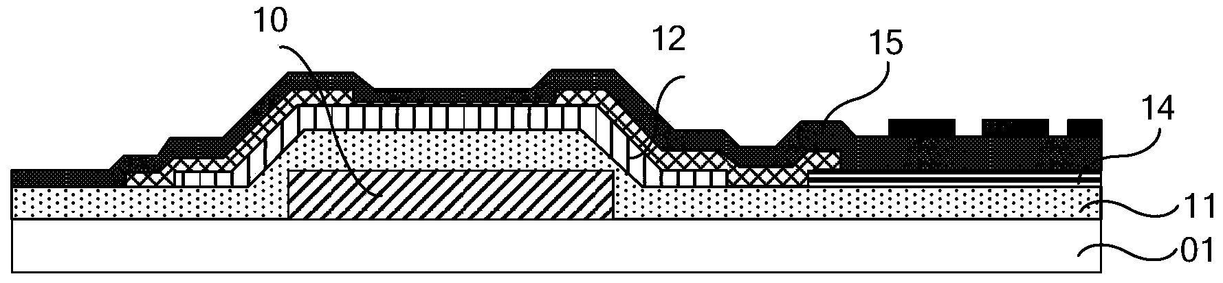
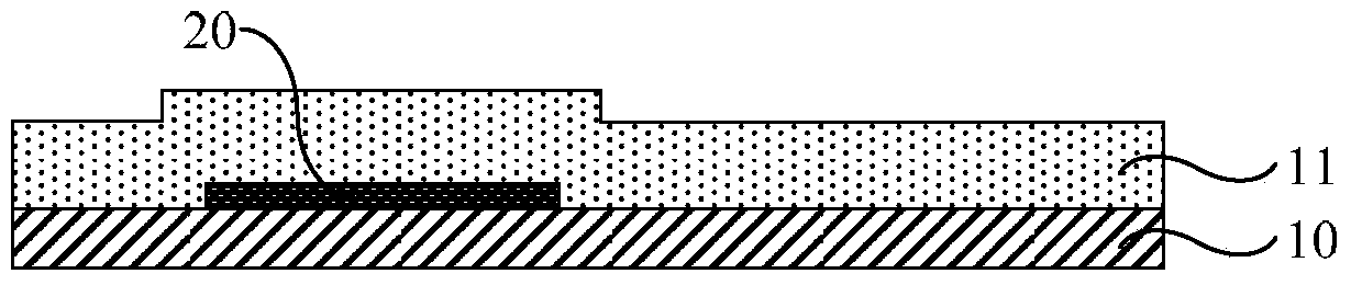
[0028] An embodiment of the present invention provides a substrate, such as Figure 4 As shown, it may include a first film layer 21 and a second film layer 22 located on the surface of the first film layer 21 ; there is at least one alignment mark 20 between the first film layer 21 and the second film layer 22 .

[0029] Wherein, the thickness H of the second film layer 22 corresponding to the position corresponding to the position mark 20 may be smaller than...


PUM


Abstract

The embodiment of the invention provides a substrate, an alignment mark manufacturing method thereof and a display device, and relates to the display technical field. With the substrate, the alignment mark manufacturing method thereof and the display device of the invention adopted, the visibility of the alignment mark can be improved. The substrate includes a first film layer and a second film layer positioned on the surface of the first film layer; at least one alignment mark exists between the first film layer and the second film layer; and the thickness of a portion of the second film layer which is corresponding to the position of the alignment mark is smaller than the thickness of portions of the second film layer which are corresponding to positions except the position of the alignment mark.

Description

technical field [0001] The present invention relates to the field of display technology, in particular to a manufacturing method of a substrate and an alignment mark thereof, and a display device. Background technique [0002] TFT-LCD (Thin Film Transistor Liquid Crystal Display, Thin Film Transistor Liquid Crystal Display), as a flat panel display device, has become more and more popular due to its small size, low power consumption, no radiation and relatively low production cost. It is widely used in the field of high-performance display. [0003] TFT-LCD consists of an array substrate, a color filter substrate, and liquid crystals filled between the array substrate and the color filter substrate. Among them, the array substrate and the color filter substrate have the characteristics of multiple film layers. For example, for array substrates, such as figure 1 As shown, it may include a gate 10 , a gate insulating layer 11 , an active layer 12 , a TFT structure, a pixel ...

Claims


Application Information

Patent Timeline
Patent Type & Authority Applications(China)
IPC IPC(8): H01L23/544H01L21/02H01L21/67
Inventor 杨光宋亚歌于光光
Owner BEIJING BOE OPTOELECTRONCIS TECH CO LTD
Why Eureka
Try Eureka