Method for producing a conversion element, and conversion element
A technology for converting components and components, applied in electrical components, chemical instruments and methods, semiconductor devices, etc., and can solve the problem of high cost
- Summary
- Abstract
- Description
- Claims
- Application Information
AI Technical Summary
Problems solved by technology
Method used
Image
Examples
Embodiment Construction
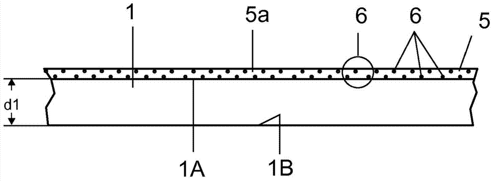
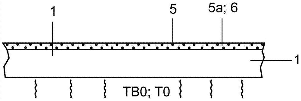
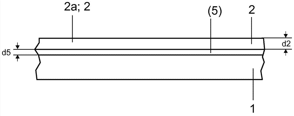
[0018] Figures 1A to 1G Various method steps of an exemplary embodiment of the method are described, wherein a schematic partial cross-sectional view of the transparent base layer 1 and further layers already arranged thereon is shown in each case. Dimensional relationships, especially layer thickness relationships, are not to scale. In addition according to Figure 1A with 1B The method steps are optional and thus can be omitted; correspondingly can also be omitted in Figures 1C to 1F Layer 5 in . From this practical approach to Figure 1C Initially, the glass solder 2a that is not yet phosphorescent is deposited or coated in another way—either directly on the transparent base layer 1 or (as shown) previously applied to the base layer 1, which can On the selected scattering layer 5.
[0019] According to an improved scheme, the scattering layer 5 ( Figure 1A ) is first deposited directly on a (preferably planar and plane-parallel) transparent substrate 1 of substrate t...
PUM
| Property | Measurement | Unit |
|---|---|---|
| softening point | aaaaa | aaaaa |
| diameter | aaaaa | aaaaa |
| softening point | aaaaa | aaaaa |
Abstract
Description
Claims
Application Information


