Embedded touch array substrate and liquid crystal display panel
An array substrate and embedded technology, applied in the fields of optics, instruments, electrical digital data processing, etc., can solve the problem of reduced touch sensitivity and achieve the effects of improving touch sensitivity, reducing power consumption, and reducing interference
- Summary
- Abstract
- Description
- Claims
- Application Information
AI Technical Summary
Problems solved by technology
Method used
Image

Examples
Embodiment Construction
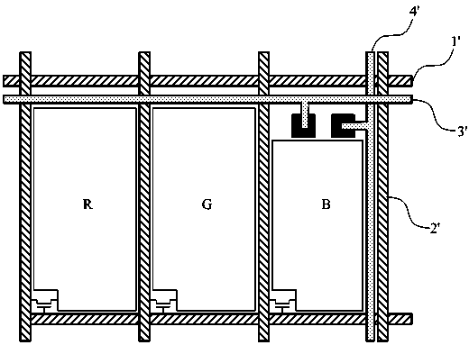
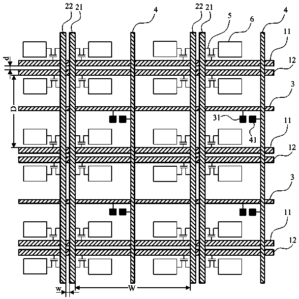
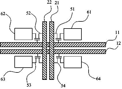
[0036] The following descriptions of various embodiments refer to the accompanying drawings to illustrate specific embodiments in which the present invention can be implemented. The terms of direction and position mentioned in the present invention, such as "upper", "middle", "lower", "front", "rear", "left", "right", "inner", "outer", "side ", etc., are only for reference to the orientation and position of the attached drawings. Therefore, the terms of direction and position are used to illustrate and understand the present invention, but not to limit the present invention.
[0037] Please refer to figure 2 As shown, Embodiment 1 of the present invention provides an in-cell touch array substrate, including:
[0038] Several pairs of grid scan lines and data lines arranged in a staggered manner;
[0039] pixel switches electrically connected to adjacent gate scanning lines and data lines;
[0040] a pixel electrode electrically connected to the pixel switch;
[0041] a t...
PUM
 Abstract
Description
Claims
Application Information
 - R&D
- Intellectual Property
- Life Sciences
- Materials
- Tech Scout
- Unparalleled Data Quality
- Higher Quality Content
- 60% Fewer Hallucinations
Browse by: Latest US Patents, China's latest patents, Technical Efficacy Thesaurus, Application Domain, Technology Topic, Popular Technical Reports.
© 2025 PatSnap. All rights reserved.Legal|Privacy policy|Modern Slavery Act Transparency Statement|Sitemap|About US| Contact US: help@patsnap.com