A multi-size wafer centering device

A centering device, multi-size technology, applied in electrical components, semiconductor/solid-state device manufacturing, circuits, etc., to achieve the effects of convenient debugging, low price, and easy installation

Active Publication Date: 2016-06-29
SHENYANG KINGSEMI CO LTD
View PDF6 Cites 1 Cited by
  • Summary
  • Abstract
  • Description
  • Claims
  • Application Information

AI Technical Summary

Problems solved by technology

The centering device solves the problem of compatible processing of wafers of different sizes, and can automatically distinguish wafers of different sizes through the manipulator according to the size of the placed cassettes to realize the centering function

Method used


Image

  • A multi-size wafer centering device
  • A multi-size wafer centering device

Examples


Embodiment Construction

[0014] The present invention will be described in further detail below in conjunction with the accompanying drawings.

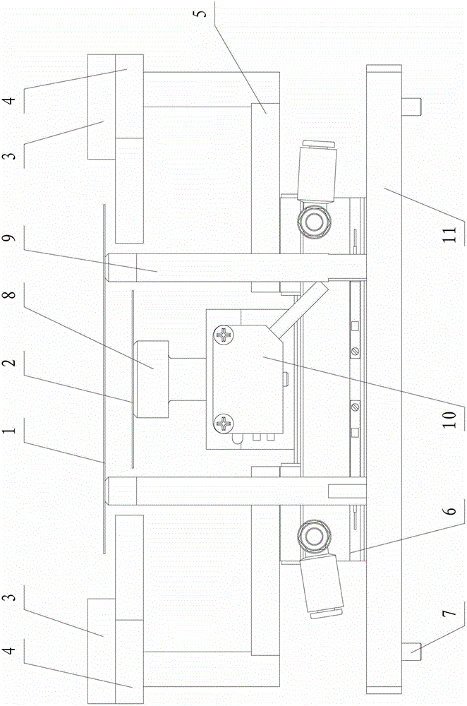
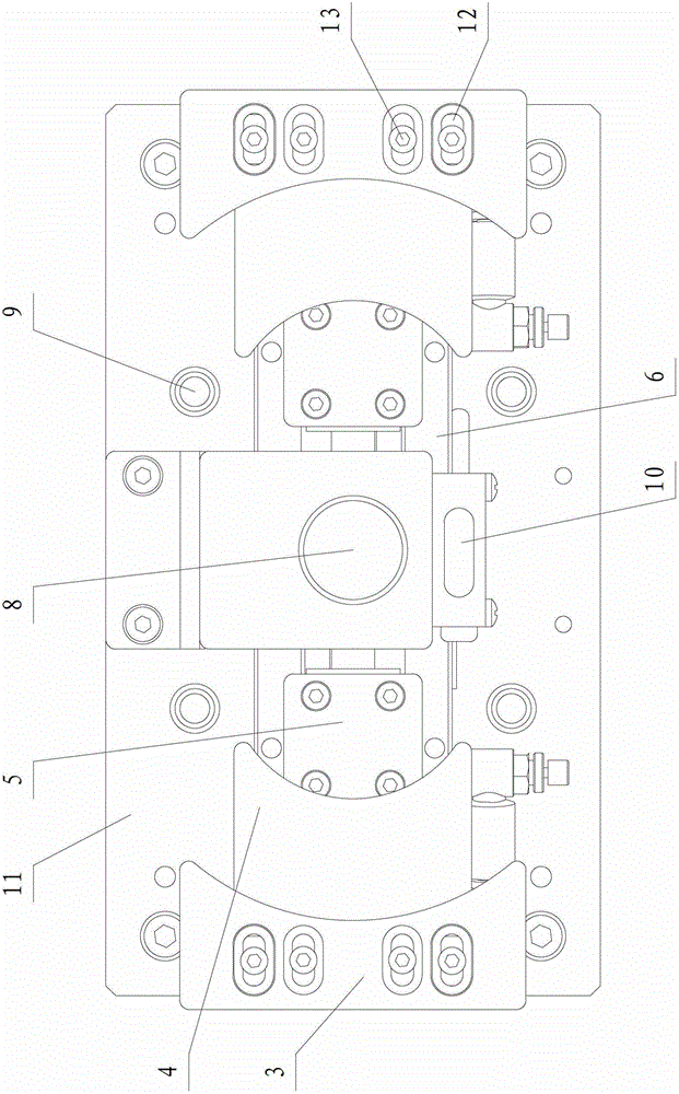
[0015] The invention is suitable for correcting the wafer position of Track equipment (glue developing equipment). The wafer position calibration is realized through the clamping action of the clamping mechanism, and wafers of different sizes can be realized through different settings of wafer support point positions. centering function. The specific structure is:

[0016] Such as figure 1 , figure 2 As shown, the present invention includes a workbench 11, a power unit, a clamping mechanism, a wafer platform 8 and a support column 9, wherein the power unit is installed on the workbench 11 and can be an air gripper 6 or an electric cylinder. The power of the present embodiment The device is air claw 6. The wafer holder 8 is installed on the workbench 11, and a plurality of support columns 9 are distributed around the wafer holder 8; the number of support ...


PUM


Abstract

The invention relates to a correction device for the positions of wafers of a semiconductor device, in particular to a centring device for the wafers of various sizes. The centring device comprises a work table, a power device, a clamping mechanism, a bearing table and supporting columns. The power device is installed on the work table, the bearing table is installed on the work table, a plurality of the supporting columns are distributed around the bearing table, and the top end of the bearing table and the top ends of the supporting columns are different in height and bear the wafers of different sizes. The clamping mechanism is connected with the output end of the power device, and the bearing table and the two sides of the supporting columns clamp the wafers inwards under driving of the power device, so that centring of the wafers is finished. The centring function is achieved by distinguishing the wafers of different sizes through the difference of supporting points of the wafers. The centring device is provided with one movement mechanism, and the pollution caused by movement friction is greatly reduced. The centring device has the advantages of being simple in structure, easy to install, convenient to adjust and low in cost, and saving the space.

Description

technical field [0001] The invention relates to a correction device for the wafer position of semiconductor equipment, in particular to a multi-size wafer centering device. Background technique [0002] At present, in order to save equipment costs, semiconductor processing plants generally require a machine capable of processing wafers of different sizes. However, the existing processing equipment is too complex in structure, bulky, and takes up a lot of space; and the wafer alignment accuracy is low, which cannot meet the processing requirements. Contents of the invention [0003] The object of the present invention is to provide a multi-size wafer centering device. The centering device solves the problem of compatible processing of wafers of different sizes, and can automatically distinguish wafers of different sizes through the manipulator according to the size of the placed cassettes to realize the centering function. [0004] The purpose of the present invention is ...

Claims


Application Information

Patent Timeline
Patent Type & Authority Patents(China)
IPC IPC(8): H01L21/68
CPCH01L21/68H01L21/6875
Inventor 张杨
Owner SHENYANG KINGSEMI CO LTD
Why Eureka
Try Eureka