Composite electrode and preparation method thereof

A composite electrode and electrode substrate technology, which is applied in the manufacture of circuits, electrical components, semiconductors/solid-state devices, etc., can solve problems such as increasing the contact area, and achieve the effects of enhancing surface effects, increasing surface area and surface energy, and making the preparation process compatible

Inactive Publication Date: 2014-05-07
BEIJING INST OF NANOENERGY & NANOSYST
View PDF8 Cites 14 Cited by
  • Summary
  • Abstract
  • Description
  • Claims
  • Application Information

AI Technical Summary

Problems solved by technology

[0002] In semiconductor devices, the surface structure of the electrode has an important impact on the performance of the device. Usually, the surface formed naturally when the electrode material is prepared is in contact with other parts of the device. Since the electrode surface formed in this way is a flat surface, it cannot meet the needs of the rough electrode surface. The need to increase the contact area when the electrode contacts or rubs with other materials

Method used


Image

  • Composite electrode and preparation method thereof
  • Composite electrode and preparation method thereof
  • Composite electrode and preparation method thereof

Examples


Embodiment Construction

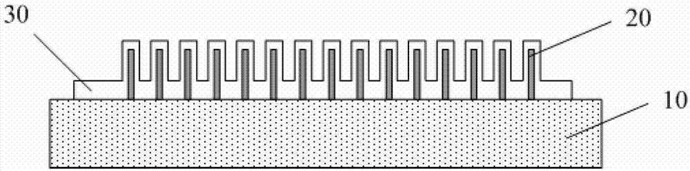
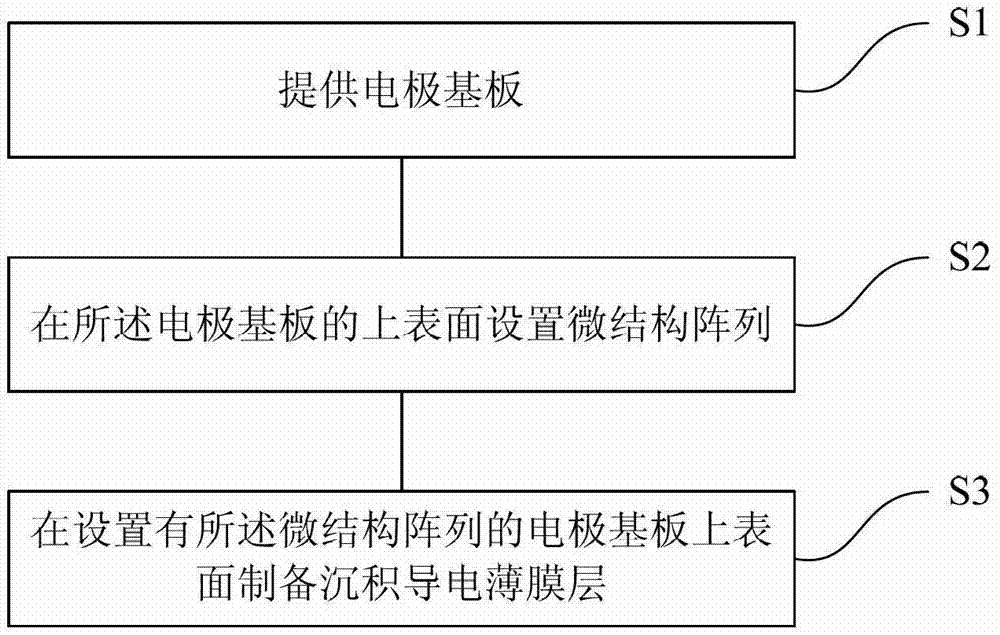
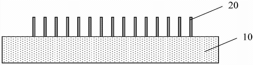
[0030] In semiconductor devices, the surface structure of the electrode has an important impact on the performance of the device. Usually, the surface formed naturally when the electrode material is prepared is in contact with other parts of the device. Contact or friction devices cannot meet the need to increase the contact area when the electrode contacts or rubs with other materials.

[0031] The invention provides a composite electrode whose surface can be a microstructure array. The technical solution is to deposit a microstructure array on the surface of a substrate as a template, and then deposit a conductive thin film layer material to obtain an electrode with a microstructure array modification layer on the surface.

[0032] Specifically, a microstructure array can be prepared on the surface of the electrode substrate by a chemical method, and then a conductive thin film layer can be deposited by a physical method to achieve the purpose of increasing the surface roughn...


PUM

PropertyMeasurementUnit
heightaaaaaaaaaa
heightaaaaaaaaaa
thicknessaaaaaaaaaa

Abstract

The invention provides a composite electrode, which comprises an electrode substrate, a micro structure array and a conductive film layer, wherein the micro structure array is arranged on the upper surface of the electrode substrate; and the conductive film is deposited on the surface of the electrode substrate provided with the micro structure array. Correspondingly, the invention further provides a preparation method for the composite electrode. According to the invention, a surface modification layer provided with the micro structure layer is prepared on the surface of the electrode substrate, thereby enabling the electrode surface to have the micro structure array, and being capable of effectively increasing the mutual contact area when the composite electrode and other materials are contacted or friction is generated therebetween.

Description

technical field [0001] The invention relates to the field of semiconductor devices, in particular to a composite electrode and a preparation method thereof. Background technique [0002] In semiconductor devices, the surface structure of the electrode has an important impact on the performance of the device. Usually, the surface formed naturally when the electrode material is prepared is in contact with other parts of the device. Since the electrode surface formed in this way is a flat surface, it cannot meet the needs of the rough electrode surface. It is necessary to increase the contact area when the electrode contacts or rubs with other materials. Contents of the invention [0003] The invention provides a compound electrode with a simple structure and a microstructure array on its surface, comprising: [0004] electrode substrate; [0005] a microstructure array arranged on the upper surface of the electrode substrate; [0006] A conductive thin film layer deposite...

Claims


Application Information

Patent Timeline
Patent Type & Authority Applications(China)
IPC IPC(8): H01L29/41H01L21/28
CPCH01L29/413H01L21/28506H01L29/401
Inventor 杨维清王中林
Owner BEIJING INST OF NANOENERGY & NANOSYST
Why Eureka
Try Eureka