Touch display panel and manufacturing method thereof

A touch display panel, touch scan line technology, applied in optics, instruments, electrical and digital data processing, etc., can solve the problems of signal delay, resistance increase, etc.

Inactive Publication Date: 2014-05-14
BOE TECH GRP CO LTD
View PDF5 Cites 35 Cited by
  • Summary
  • Abstract
  • Description
  • Claims
  • Application Information

AI Technical Summary

Problems solved by technology

In order to obtain higher touch accuracy, it is necessary to reduce the line width of the touch scanning line and the touch sensing line, but this will cause the resistance value of the touch scanning line and the to

Method used


Image

  • Touch display panel and manufacturing method thereof
  • Touch display panel and manufacturing method thereof
  • Touch display panel and manufacturing method thereof

Examples


preparation example Construction

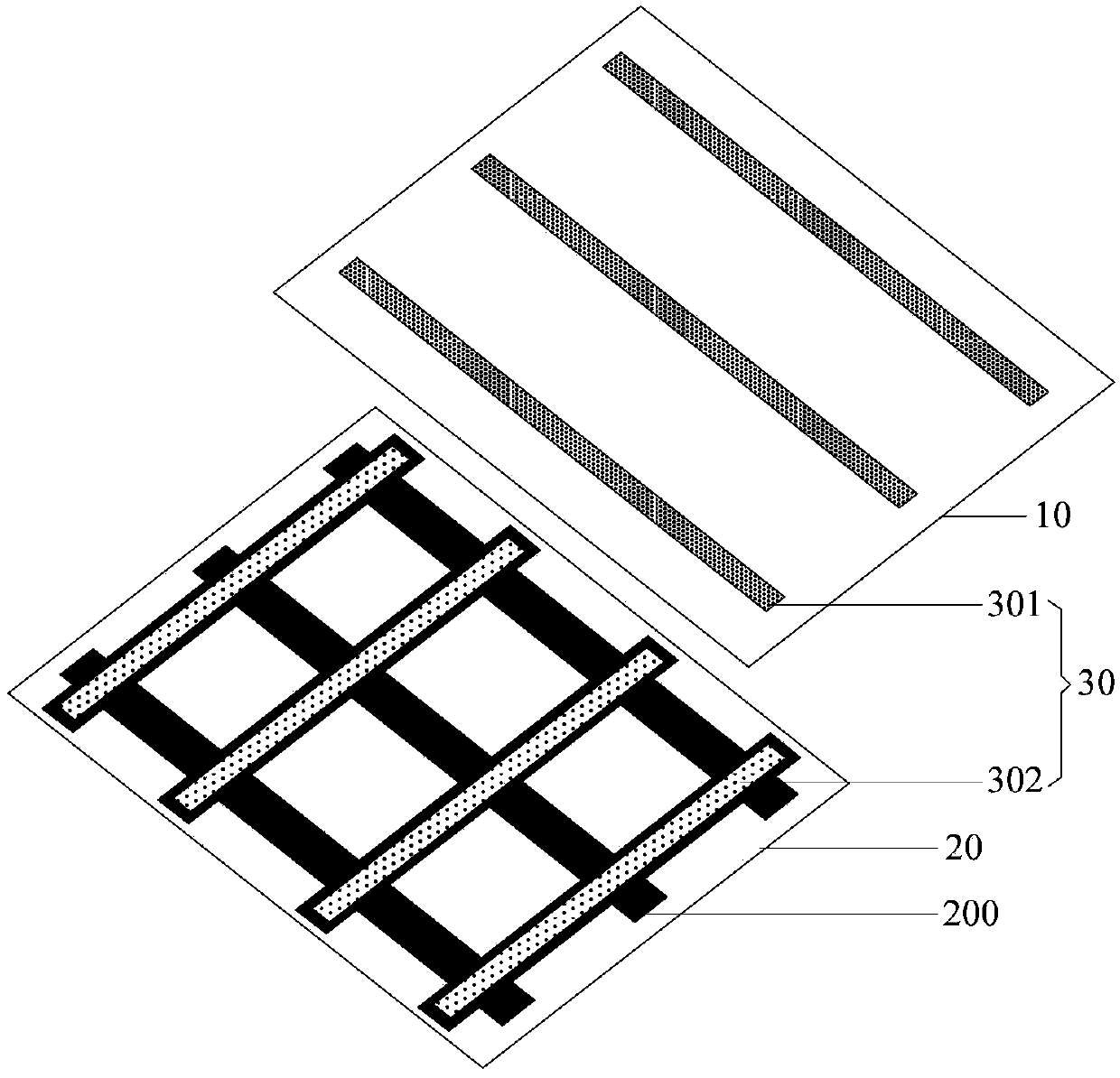
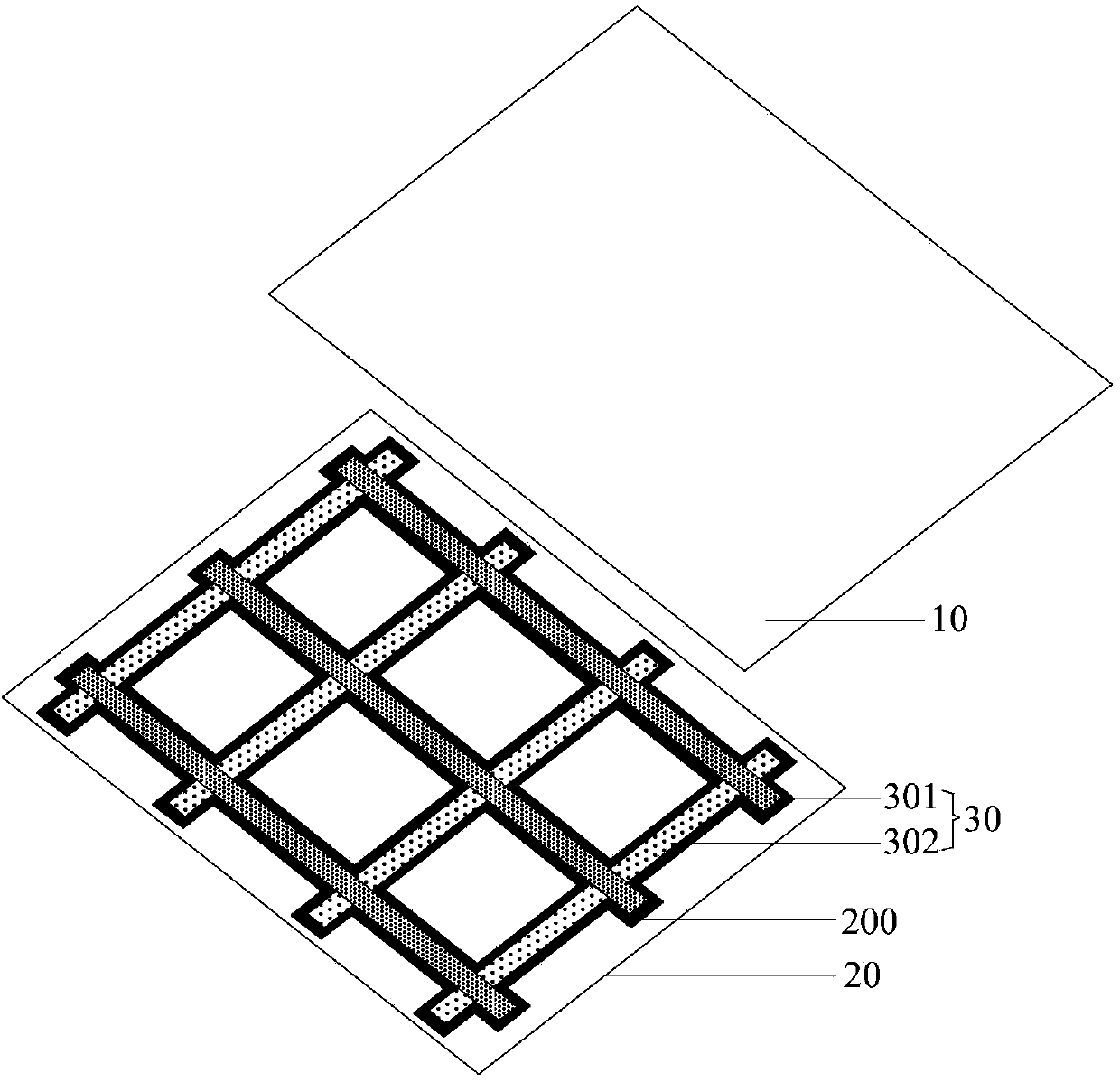
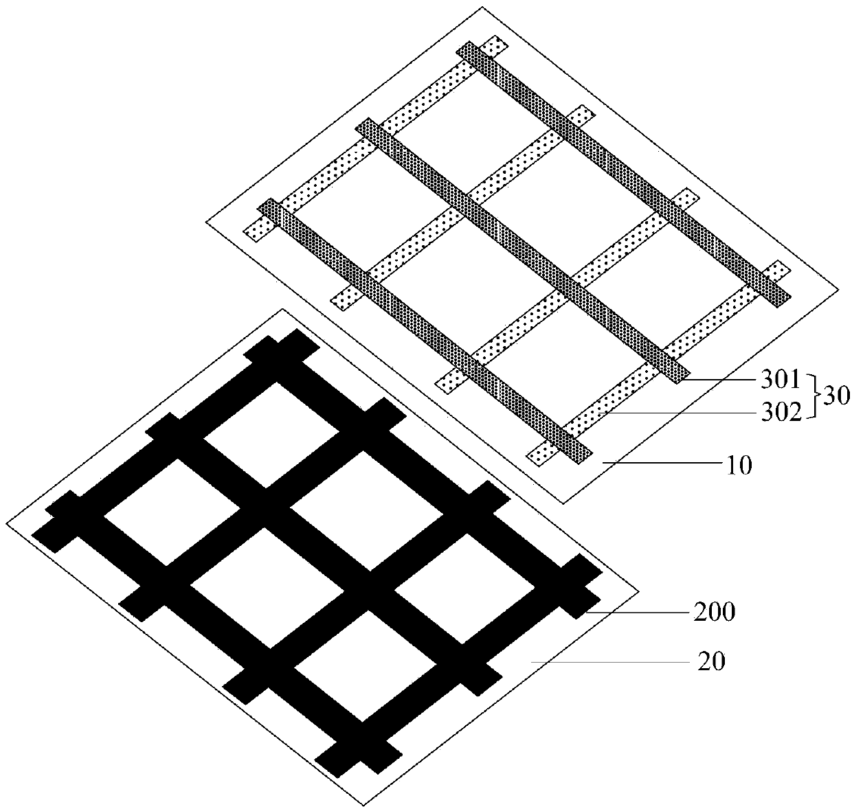
[0055] The embodiment of the present invention also provides a method for manufacturing the above touch display panel, the method includes: when forming the first electrode line 301 and / or the second electrode line 302 corresponding to the position of the black matrix 200, low temperature deposition A metal layer is formed by a process, and then a mask process is performed on the metal layer to form a metal electrode line.

[0056] Wherein, the low-temperature deposition process may be a deposition process performed by a low-temperature magnetron sputtering method; on this basis, preferably, a thickness of 100° C. can be formed by a magnetron sputtering process under an atmosphere of 20°C to 50°C. ~400nm of the metal layer.

[0057] On this basis, refer to figure 2 with image 3 As shown, the first electrode lines 301 and the second electrode lines 302 may both be formed on the color filter substrate 20 or both may be formed on the array substrate 10; wherein, the first electrode ...


PUM

PropertyMeasurementUnit
Thicknessaaaaaaaaaa

Abstract

Embodiments of the invention provide a touch display panel and a manufacturing method thereof, relate to the technical field of touch displaying and aim to reduce resistance of touch electrodes, improve signal lag and increase touch precision accordingly. The touch display panel comprises an array substrate and a color film substrate abutted to each other. The touch display panel further comprises a group of parallel first electrode lines arranged on the array substrate or the color film substrate, and a group of parallel second electrodes; the second electrode lines arranged on the array substrate or the color film substrate intersect with the first electrode lines for arraignment; the first electrode lines are non-electrically connected with the second electrode lines. The first electrode lines and/or the second electrode lines correspond to a black array of the color film substrate in position; the first electrode lines and/or the second electrode lines corresponding to the black array in position are metal electrode lines. The touch display panel and the manufacturing method thereof are applicable to manufacturing of touch display devices.

Description

Technical field [0001] The present invention relates to the technical field of touch display, in particular to a touch display panel and a preparation method thereof. Background technique [0002] With the continuous development of display technology, the research on the integration of touch panel functions and liquid crystal display panels has become increasingly popular. [0003] At present, the integrated technology research and development route of the in-cell touch screen mainly includes on-cell touch and in-cell touch. The difference between the two is: on-cell touch is a touch technology that embeds the touch panel function between the color film substrate and the polarizing plate. Specifically, the touch sensor component layer in the touch panel is made on On the base substrate and bonded with the color filter, so as to be embedded in the liquid crystal pixel; in-cell touch is a touch technology that embeds the touch panel function into the liquid crystal pixel, specifical...

Claims


Application Information

Patent Timeline
IPC IPC(8): G02F1/1333
CPCG06F3/0412G06F3/0445G06F3/0446G06F2203/04103G06F2203/04112G06F3/047
Inventor 王灿王路
Owner BOE TECH GRP CO LTD
Why Eureka
Try Eureka