
Semiconductor device

A technology of semiconductors and transistors, which is applied in the field of semiconductor devices and can solve problems such as difficulties in the layout of NMOS transistors

Active Publication Date: 2014-05-14
SII SEMICONDUCTOR CORP
View PDF7 Cites 3 Cited by
  • Summary
  • Abstract
  • Description
  • Claims
  • Application Information

AI Technical Summary

Problems solved by technology

[0007] However, the surge current of ESD is extremely large and instantaneous
Therefore, it is very difficult to specify the layout of NMOS transistors according to this surge current
On the contrary, it is practically impossible to quantify the dependence of ESD tolerance on the layout of NMOS transistors

Method used


Image

  • Semiconductor device
  • Semiconductor device
  • Semiconductor device

Examples


no. 1 approach

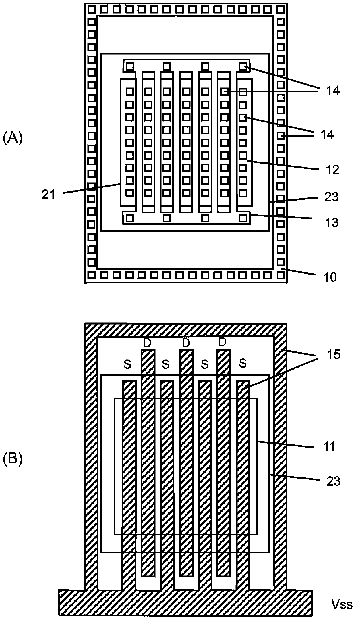
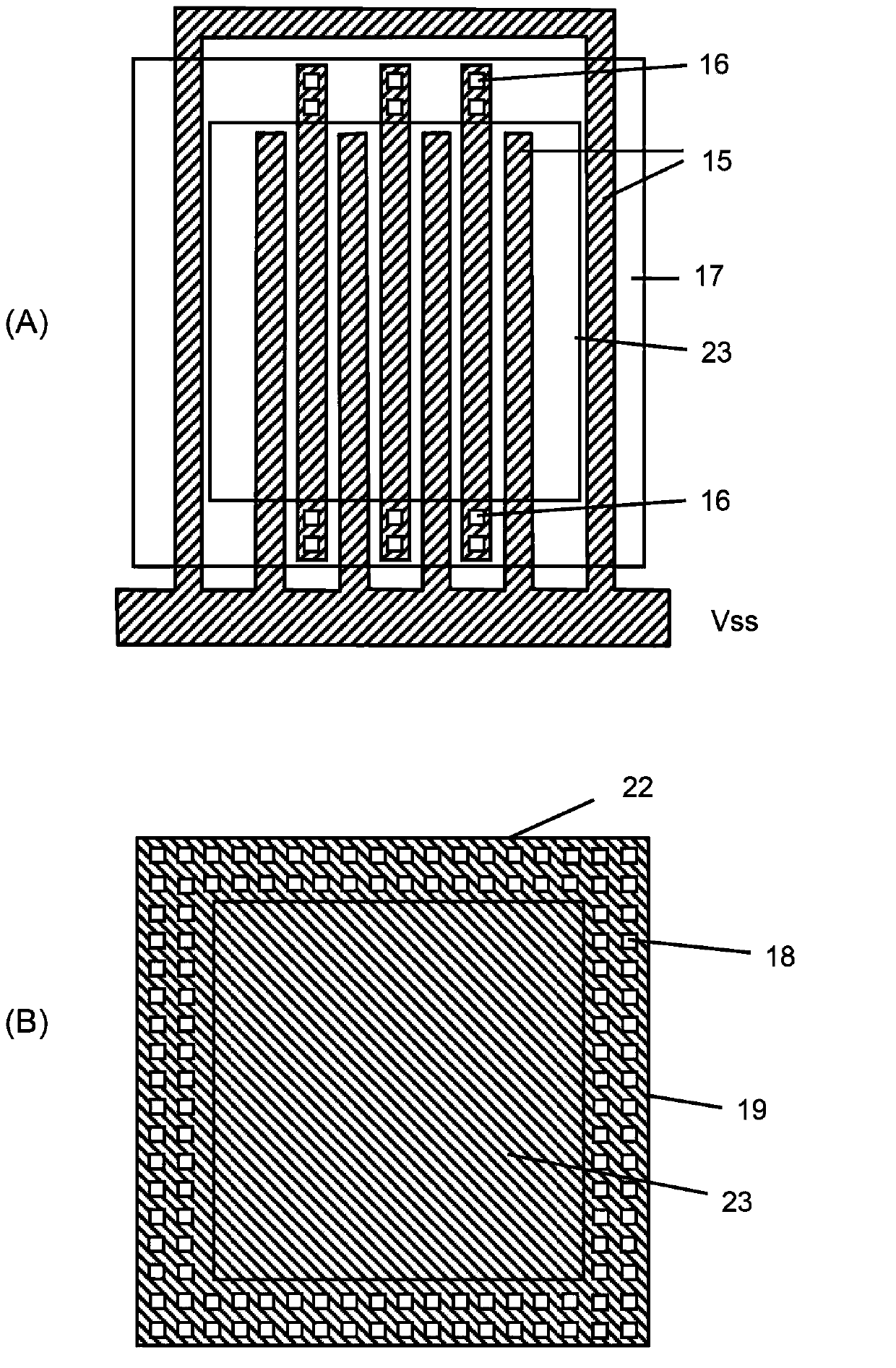
[0021] First, use figure 1 with figure 2 The pad structure of the semiconductor device will be described. figure 1 It is a plan view showing a pad structure of a semiconductor device, (A) shows a diffusion region, a gate electrode, a contact, and a pad opening, and (B) shows a diffusion region, an underlying metal film, and a pad opening. figure 2 is shown with figure 1 The top view of the pad structure of the same semiconductor device, (A) shows the lower metal film, the first via hole, the middle metal film and the pad opening, (B) shows the second via hole, the upper metal film and the pad opening. Disk opening.

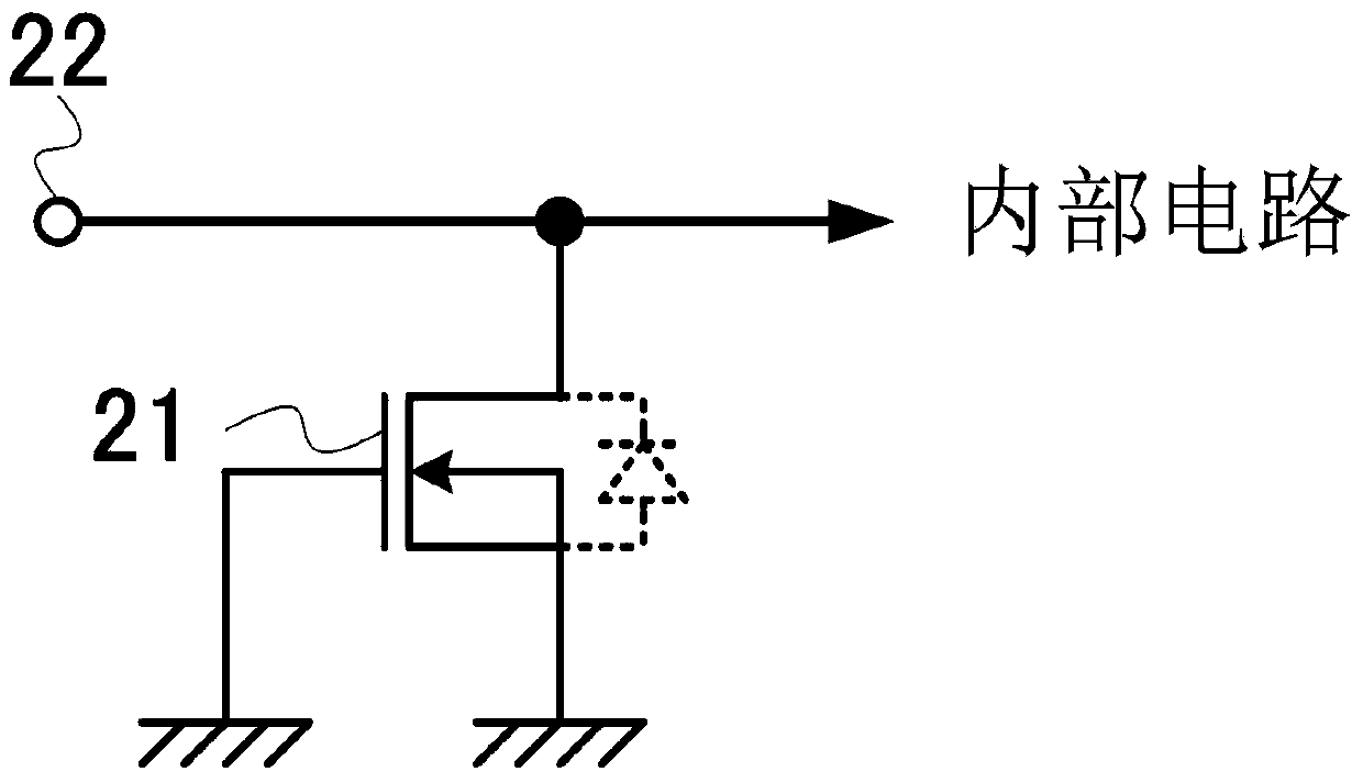
[0022] Such as figure 1 As shown in (A), a P-type diffusion region 10 for fixing the substrate potential and an N-type diffusion region 12 for the source and drain are provided, and a gate electrode is provided between the N-type diffusion regions 12 for the source and drain 13, constituting the NMOS transistor 21. The NMOS transistor 21 is a multi-finger ...


PUM


Abstract

Provided is a semiconductor device having high ESD tolerance. A first via (16) is used for electrically connecting a pad (22) to a drain of an NMOS transistor of an ESD protective circuit. The first vias (16) are formed under the pad (22) only on one side of a rectangular ring-shaped intermediate metal film (17) and on another side thereof opposed to the one side. In other words, all the first vias (16) for establishing an electrical connection to the drains are present substantially directly under the pad (22). Consequently, a surge current caused by ESD and applied to the pad (22) is more likely to flow uniformly among all the drains. Then, respective channels of the NMOS transistor of the ESD protective circuit are more likely to uniformly operate, and hence the ESD tolerance of the semiconductor device is increased.

Description

technical field [0001] The present invention relates to a semiconductor device having an NMOS transistor under a bonding pad. Background technique [0002] A semiconductor device called an IC or a semiconductor chip has pads as electrodes for external connection in order to be electrically connected to other elements or other semiconductor devices. An ESD protection circuit that protects the internal circuit of the semiconductor device from ESD (Electrostatic Discharge) is generally provided near the pad. Multi-finger NMOS transistors are mostly used in ESD protection circuits. At this time, the gate electrode, source, and back gate of the NMOS transistor are connected to the ground terminal, and the drain is connected to the pad. [0003] Here, in the ESD protection circuit using multi-finger NMOS transistors, various methods have been tried, and each channel operates in unison, and the ESD tolerance of the semiconductor device becomes high. Specifically, for example, in...

Claims


Application Information

Patent Timeline
Patent Type & Authority Applications(China)
IPC IPC(8): H01L23/58H01L23/60
CPCH01L2924/0002H01L23/4824H01L27/0251H01L29/41758H01L2924/00
Inventor 小山威广濑嘉胤
Owner SII SEMICONDUCTOR CORP
Learn More