
Semiconductor integrated circuit

An integrated circuit and semiconductor technology, applied in the field of semiconductor integrated circuits, can solve the problems of slow switching speed of transistors, damage to gate oxide film, hindering the speed of output circuit, etc., and achieve the effect of preventing ESD damage, small resistance, and fast action.

Inactive Publication Date: 2005-02-09
NEC ELECTRONICS CORP
View PDF4 Cites 9 Cited by
  • Summary
  • Abstract
  • Description
  • Claims
  • Application Information

AI Technical Summary

Problems solved by technology

[0010] In the above-mentioned first prior art example, since the parasitic capacitance of the drain region increases due to the N well provided in the drain region of the output transistor, the switching speed of the transistor becomes slow, and there is a problem that it is impossible to speed up the output circuit.
In the second prior art example, the ESD current flows due to the operation of the parasitic bipolar transistor of the protection element, so when the diffusion layer is silicided, it is necessary to take the same countermeasures as in the first prior art example. There is a problem that the speed of the output circuit cannot be realized
Also, in the second prior art example, the gate electrode of the always-on NMOS transistor is connected to the power supply terminal VDD, so there is a concern that the gate oxide film may be damaged by an ESD strike between the output terminal and the power supply terminal.
Especially in the cutting-edge CMOS technology of the 90nm node with a gate oxide film of about 1.6nm, it is also essential to provide a protection circuit between the output terminal and the power supply terminal, so the protection circuit between the output terminal and the power supply terminal produces The parasitic capacitance also hinders the rapidity of the output circuit

Method used


Image

  • Semiconductor integrated circuit
  • Semiconductor integrated circuit
  • Semiconductor integrated circuit

Examples


Embodiment Construction

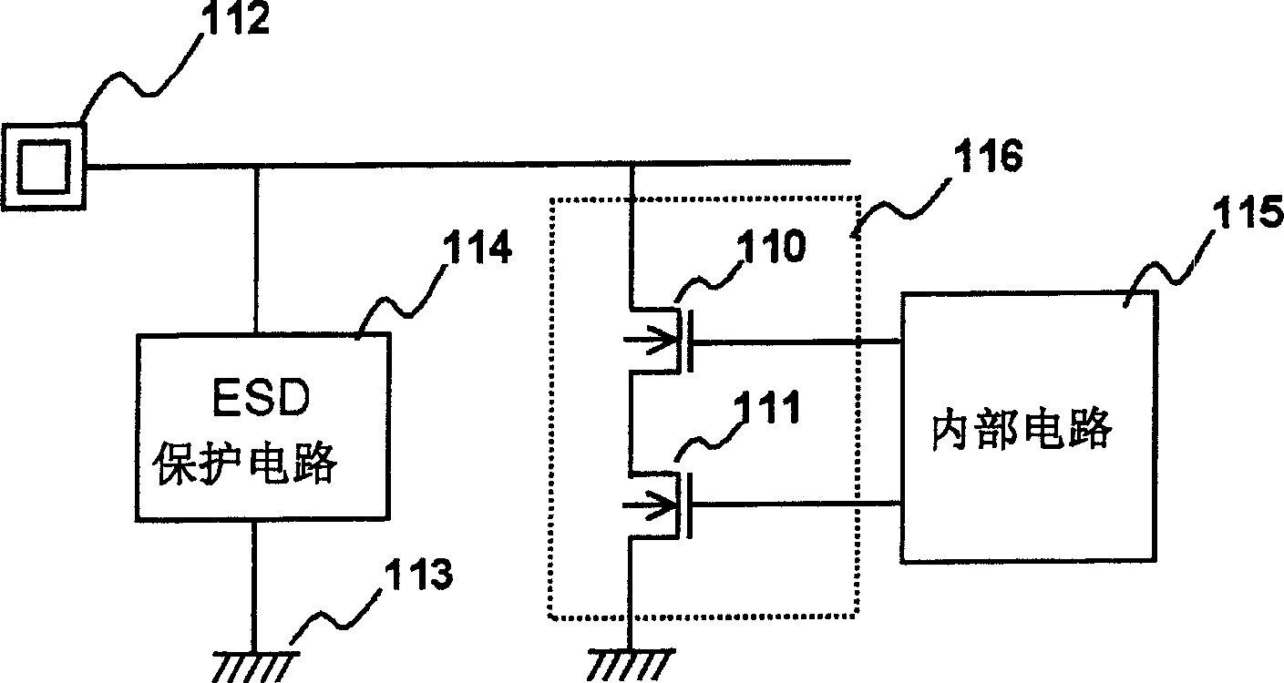
[0026] Hereinafter, the first embodiment of the present invention will be described with reference to the drawings. figure 1 It is a circuit diagram showing the main components of the first embodiment. in figure 1 Here, 112 denotes the output terminal of the semiconductor integrated circuit. 114 denotes a dedicated ESD protection circuit provided between the output terminal 112 and the ground terminal 113, and 115 denotes an internal circuit. 110 is a first NMOS transistor, and 111 is a second NMOS transistor, which are connected in cascade. The first NMOS transistor 110 and the second NMOS transistor 111 constitute an output circuit 116 for outputting a signal of the internal circuit 115, and the gate electrodes of the first NMOS transistor 110 and the second NMOS transistor 111 are both connected to the internal circuit 115.

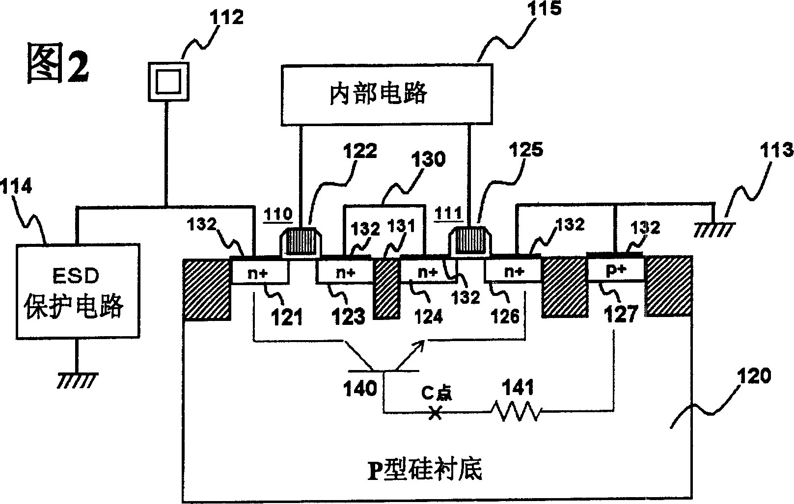
[0027] Fig. 2 is a cross-sectional view showing main components of the first embodiment. A first NMOS transistor 110 and a second NMOS transistor 111 are...


PUM


Abstract

To provide an output circuit having a low parasitic capacitance and resistance in the drains of output transistors, which is operable at a high speed and its ESD performance is improved. A devoted electrostatic discharge protection circuit is provided between the output terminal (pin) and the ground terminal (or power supply terminal). An output circuit which is in parallel connected to this electrostatic discharge protection circuit comprises a first and second MOS transistors which are cascade-connected to each other. The entire area of the source / drain regions of the first and second MOS transistors are silicided. Both transistors have their gate electrodes which are connected to an internal circuit. The source doped region of the first MOS transistor is separated from the drain doped region of the second MOS transistor and they are connected to each other by metal wiring.

Description

Technical field [0001] The present invention relates to a semiconductor integrated circuit, in particular to a semiconductor integrated circuit having a fast output circuit with enhanced antistatic properties. Background technique [0002] MOS transistors constituting semiconductor integrated circuits have been increasingly miniaturized in recent years. With the thinning of the thinner gate insulating film and the shallower junction of the PN junction, the electrostatic protection (ESD protection) of semiconductor integrated circuits is becoming more and more difficult. In order to prevent electrostatic damage, it is indispensable to improve the performance of the ESD protection circuit. of. [0003] With the advancement of miniaturization, in order to make the source and drain diffusion layers low resistance, a technology that uses cobalt silicide or titanium silicide to apply silicidation to the diffusion layer is introduced. However, in MOS transistors that have been subjected...

Claims


Application Information

Patent Timeline
Patent Type & Authority Applications(China)
IPC IPC(8): H01L27/04H01L21/822H01L21/8234H01L23/60H01L23/62H01L27/02H01L27/06H01L27/07H01L27/088H03K19/0175
CPCH01L2924/0002H01L23/60H01L27/088H01L27/0716H01L2924/3011H01L27/0266H01L2924/00H03K19/0175
Inventor 森下泰之
Owner NEC ELECTRONICS CORP
Learn More