Method for alarm centralized processing for semiconductor processing device

A processing equipment and centralized processing technology, applied in the direction of comprehensive factory control, comprehensive factory control, electrical program control, etc., can solve the problems of inconvenient alarm management, difficulty in adding or deleting alarms, etc., and achieve the effect of convenient management

Active Publication Date: 2014-05-21
BEIJING NAURA MICROELECTRONICS EQUIP CO LTD
View PDF5 Cites 12 Cited by
  • Summary
  • Abstract
  • Description
  • Claims
  • Application Information

AI Technical Summary

Problems solved by technology

[0006] ①. Since the same alarm may affect multiple modules, this causes the same alarm to be declared and registered repeatedly in different modules;
[0007] ②. The management an

Method used


Image

  • Method for alarm centralized processing for semiconductor processing device
  • Method for alarm centralized processing for semiconductor processing device
  • Method for alarm centralized processing for semiconductor processing device

Examples


Embodiment Construction

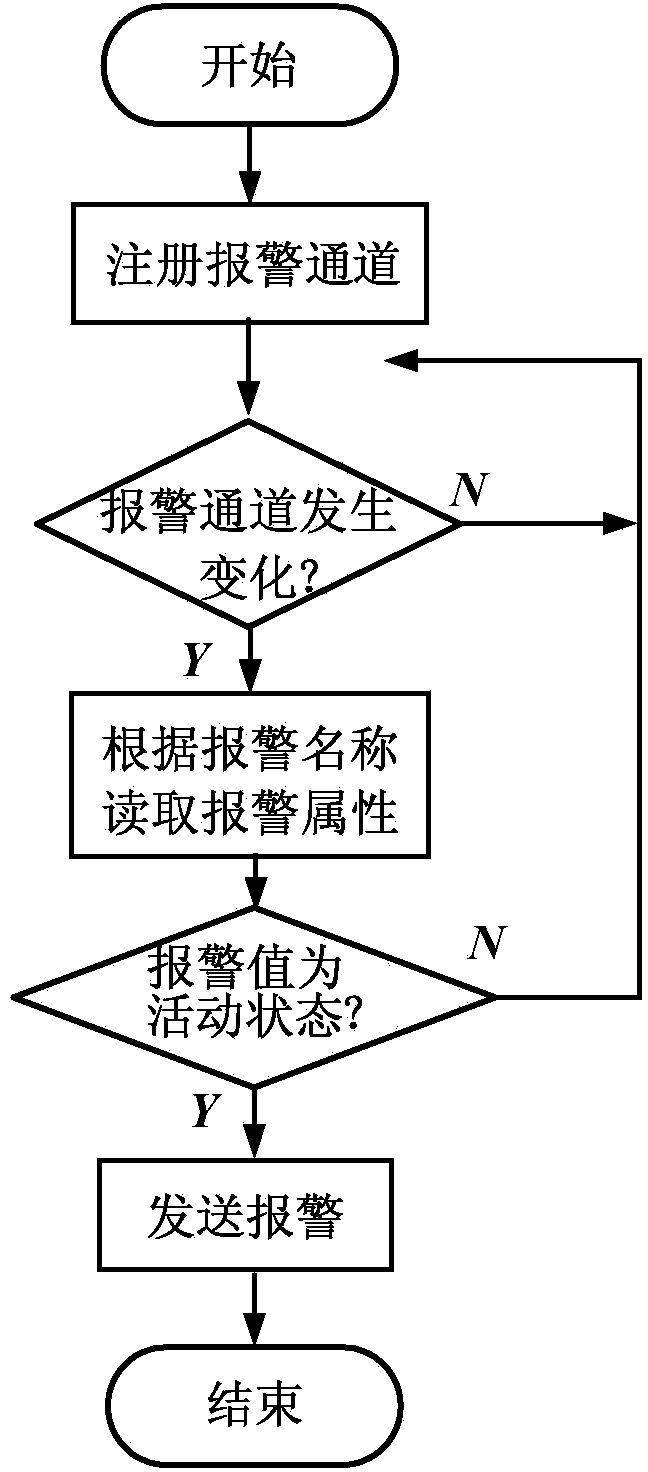
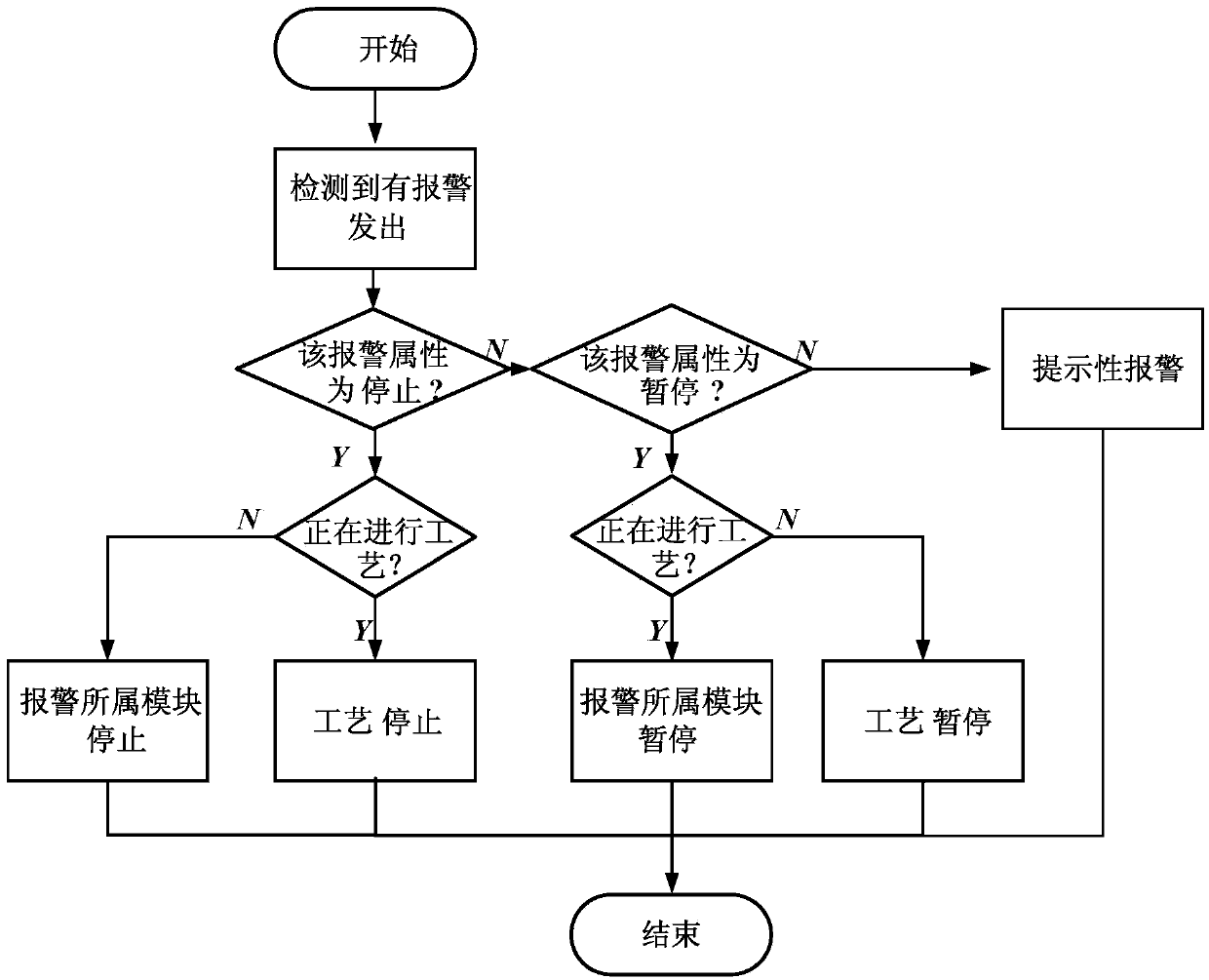
[0033] Attached below Figure 1-3 , the specific embodiment of the present invention will be further described in detail.

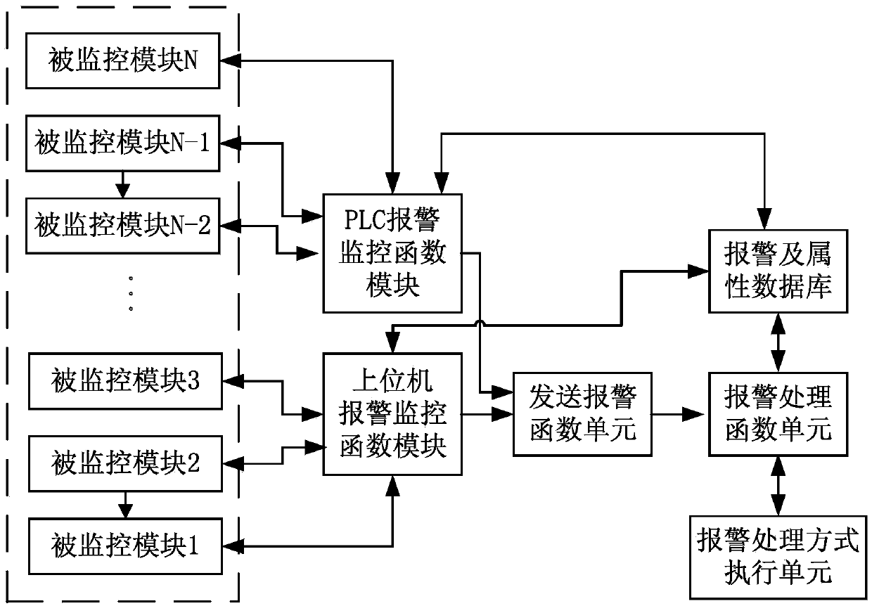
[0034] see figure 1 , figure 1 It is a structural schematic diagram of a preferred embodiment of the centralized alarm processing system for semiconductor processing equipment of the present invention. In this embodiment, multiple monitored modules may be included in the semiconductor processing equipment, for example, figure 1 N of them, N is a positive integer greater than 1; the execution structure of the monitoring system is usually a structure of upper computer + lower computer, wherein the lower computer is a programmable controller (Programmable Logic Device, PLD for short). Same as the prior art, the monitored module can be monitored by the upper computer and / or the lower computer and obtain alarm information.

[0035] Unlike existing technologies, such as figure 1 As shown, the monitoring system also includes an alarm attribute database, a P...


PUM


Abstract

A method for alarm centralized processing for a semiconductor processing device comprises the steps of adopting a database to set and store all alarms and attributes of the alarms, and enabling the attributes to comprise alarm number attributes, alarm name attributes, alarm level attributes, alarm constraint attributes, alarm processing mode attributes, PLC alarm channel addresses, attributes of monitored modules where the alarms are located and/or alarm recovery attributes; reading all the alarms and the attributes of the alarms in the database and registering PLC alarm monitoring; if alarm events occur in a PLC part, entering a PLC alarm monitoring function module to read associated attributes of the alarm events, calling alarm sending functions and giving an alarm to an upper computer; if alarm events occur in the upper computer, entering upper computer alarm monitoring functions to read associated attributes of the alarm events, calling the alarm sending functions and giving an alarm; finally, selecting a corresponding alarm recovery mode to perform alarm processing according to the processing mode attributes of the alarms in the database corresponding to alarm processing functions.

Description

technical field [0001] The invention relates to the technical field of integrated circuit manufacturing, and more specifically relates to a centralized alarm processing method for semiconductor processing equipment. Background technique [0002] At present, the design of semiconductor devices is developing rapidly in the direction of high density and high integration, which puts forward higher and higher requirements for heat treatment equipment of semiconductor equipment. Due to the complex structure and huge system of semiconductor heat treatment equipment, and the high value of its products (wafers). Therefore, in the semiconductor manufacturing process, users hope that heat treatment equipment can run multiple processes continuously for a long time without failure, which puts forward high requirements on the stability of the equipment. [0003] In order to meet the high requirements for the safety and stability of semiconductor processing equipment in the process, it is...

Claims


Application Information

Patent Timeline
IPC IPC(8): G05B19/418
CPCY02P90/02
Inventor 王亚宁郑思远钟结实张立超
Owner BEIJING NAURA MICROELECTRONICS EQUIP CO LTD
Why Eureka
Try Eureka