Semiconductor device, method of manufacturing semiconductor device, and antenna switch module

A semiconductor and device technology, applied in the field of semiconductor device manufacturing methods and antenna switch modules, can solve the problems of n-channel MOSFET threshold voltage drop, polysilicon resistance rise, field strength rise, etc.

Active Publication Date: 2014-05-21
SONY CORP
View PDF10 Cites 195 Cited by
  • Summary
  • Abstract
  • Description
  • Claims
  • Application Information

AI Technical Summary

Problems solved by technology

[0015] However, in recent years, since the technology for achieving higher power output has been advanced and the field strength has been increased, it may not be sufficient to provide a crystal defect layer only on one side of the semiconductor substrate in some cases
In this case, an electron beam irradiation method that allows crystal defects to be introduced uniformly over the entire surface of the substra...

Method used


Image

  • Semiconductor device, method of manufacturing semiconductor device, and antenna switch module
  • Semiconductor device, method of manufacturing semiconductor device, and antenna switch module
  • Semiconductor device, method of manufacturing semiconductor device, and antenna switch module

Examples


no. 1 approach

[0052] (B) Second Embodiment

[0053] (C) Third Embodiment

[0054] (D) Fourth embodiment

[0055] (E) Fifth Embodiment

[0056] (F) Summary of Example Implementations

[0057] (A) First Embodiment

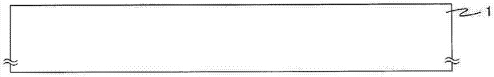
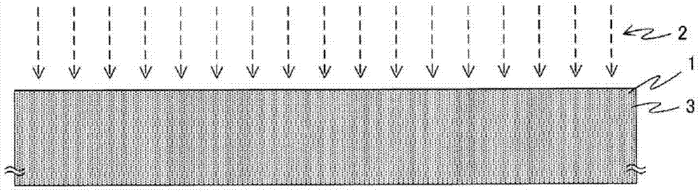
[0058] figure 1 is a flowchart showing the flow of the manufacturing method of the semiconductor device according to the first embodiment of the present disclosure, and Figure 2 to Figure 5 respectively with figure 1 Cross-sectional views of the semiconductor device corresponding to each step of the fabrication method shown in . Hereinafter, along figure 1 The flow of the fabrication method shown in provides a description.

[0059] exist figure 1 In the fabrication method shown in , as a start, prepare as figure 2 Shown is a silicon substrate 1 used as a base of a crystal defect introducing substrate ( S110 ). figure 2 is a cross-sectional view of the silicon substrate 1 .

[0060] For the silicon substrate 1, an oxygen concentration of about 1×10 produced by the FZ...


PUM


Abstract

The invention relates to a semiconductor device, a method of manufacturing semiconductor device, and an antenna switch module. Disclosed is a semiconductor device having a radio frequency switch. Also disclosed are an antenna switch module and a method of manufacturing the semiconductor device. The semiconductor device includes a metal wiring insulating film bonded to a silicon substrate. In the semiconductor device, a crystal defect layer extends into the silicon substrate from a surface of the silicon substrate. Crystal defects are throughout the crystal defect layer. The semiconductor device and an integrated circuit are in the antenna switch module. The integrated circuit in the antenna switch module is mounted with the radio-frequency switch device and the silicon substrate. The method of manufacturing the semiconductor device includes a step of forming crystal defects throughout a silicon substrate. Radiation or a diffusion is used to form the crystal defects. After the step of forming the crystal defects, the method includes a step of implanting ions into a surface of the silicon substrate to form a crystal defect layer.

Description

technical field [0001] The present disclosure relates to a semiconductor device, a manufacturing method of the semiconductor device, and an antenna switch module, and more particularly, to a semiconductor device having a radio frequency switching device on an SOI (silicon on insulator) substrate (substrate, substrate), the A manufacturing method of a semiconductor device and an antenna switch module. Background technique [0002] In recent years, for antenna switching devices, FETs (Field Effect Transistors) of compound semiconductors (for example, GaAs) that allow easy manufacture of complex switching circuits with reduced power consumption have been used. [0003] However, such compound semiconductor FETs have disadvantages in that they themselves may be relatively expensive, and they may involve high manufacturing costs due to having to be incorporated into a peripheral circuit as a module fabricated on a separate chip, or for any other reason. It is to be noted that exa...

Claims


Application Information

Patent Timeline
IPC IPC(8): H01L23/66H01L25/00H01L21/02H01L21/263
CPCH01L21/76256H01L21/76898H01L23/525H01L23/66H01L24/11H01L2224/11H01L2924/12036H01L2924/1305H01L2924/13055H01L2924/1306H01L2924/13091H01L2924/00H01L21/265H01L21/76254H01L23/481H01L27/1203H01L29/7841H01P1/15
Inventor 本山理一恒见大树山县秀夫
Owner SONY CORP
Why Eureka
Try Eureka