All-dimensional LED illumination package structure implemented by aid of transparent ceramic COB (chip on board) substrate

A technology of LED lighting and transparent ceramics, applied in lighting devices, components of lighting devices, lighting and heating equipment, etc., can solve the problems of light output and heat dissipation at small lighting angles, achieve soft light in the space, reduce heat accumulation, Reduce the effect of light attenuation

Inactive Publication Date: 2014-05-28
LUOYANG CEN LON CERAMICS
View PDF4 Cites 1 Cited by
  • Summary
  • Abstract
  • Description
  • Claims
  • Application Information

AI Technical Summary

Problems solved by technology

[0005] The purpose of the present invention is to overcome the defects existing in the heat dissipation packaging substrate used by LEDs, and provide a new packaging structure that utilizes transparent ceramic COB substrates to realize omni-directional LED lighting. The technical problem to be solved is aimed at the existing There are problems such as small lighting angle, light output and heat dissipation of LED plane or quasi-plane light source using opaque ceramic substrates, so that it can realize all-round lighting of LED, so that the lighting angle can be increased from the traditional 120° to 165° To about 270°, the light in the space is soft and uniform, and the human vision is more comfortable

Method used


Image

  • All-dimensional LED illumination package structure implemented by aid of transparent ceramic COB (chip on board) substrate
  • All-dimensional LED illumination package structure implemented by aid of transparent ceramic COB (chip on board) substrate
  • All-dimensional LED illumination package structure implemented by aid of transparent ceramic COB (chip on board) substrate

Examples


Embodiment Construction

[0020] In order to further explain the technical means and effects of the present invention to achieve the intended purpose of the invention, the following, in conjunction with the accompanying drawings and preferred embodiments, will discuss the packaging structure of the omni-directional LED lighting using a transparent ceramic COB substrate proposed according to the present invention. Specific embodiments, structures, features and effects thereof are described in detail below.

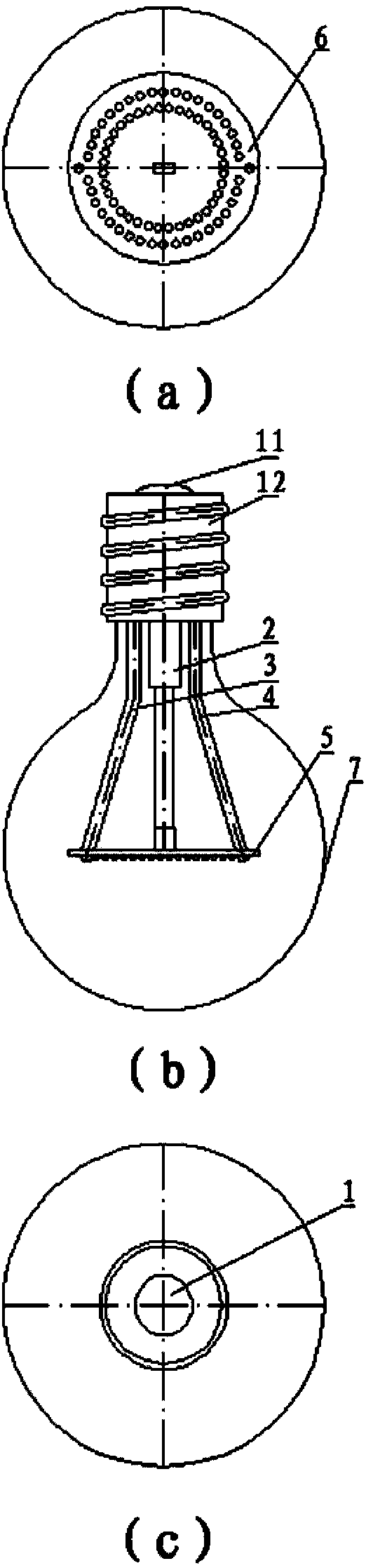
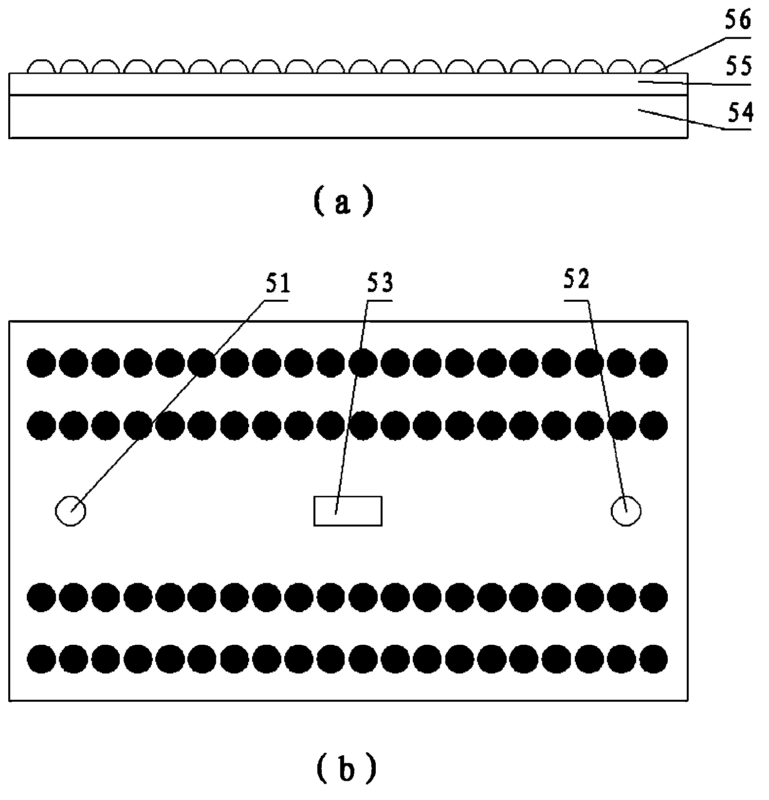
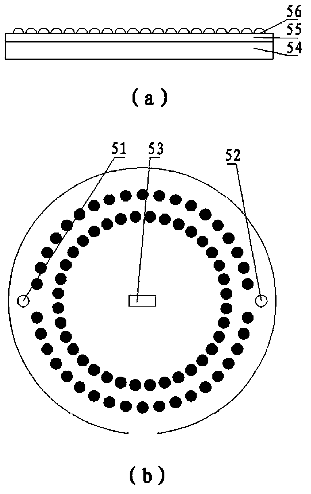
[0021] see figure 1 As shown in (a), (b), and (c), the present invention uses transparent ceramics as the structural design of the COB packaging substrate, which includes: bulb 1, positive contact 11, screw port 12 (negative contact), heat conduction column 2 , positive lead wire 3, cathode lead wire 4, transparent ceramic COB substrate 5. The upper end of the bulb 1 is provided with a screw port 12, the positive contact 11 is arranged on the top of the screw port 12 (the negative contact 12), the ...


PUM

PropertyMeasurementUnit
thicknessaaaaaaaaaa
thicknessaaaaaaaaaa

Abstract

The invention discloses an all-dimensional LED illumination package structure implemented by the aid of a transparent ceramic COB (chip on board) substrate. The all-dimensional LED illumination package structure comprises a bulb, an anode contact, a screw head, a heat conduction column, an anode wire, a cathode wire and a transparent ceramic COB chip. The transparent ceramic COB chip is respectively connected with the heat conduction column, the anode wire and the cathode wire. The transparent ceramic COB chip is of a layered structure, the transparent ceramic substrate is arranged at the bottommost layer of the transparent ceramic COB chip, a silver paste circuit layer or a copper-based circuit layer is arranged on an upper layer of the ceramic substrate, and LED chips are arranged on an upper layer of the silver paste circuit layer. Three holes are formed in the transparent ceramic COB chip and include an anode wiring hole, a cathode wiring hole and a heat conduction column mounting hole. The all-dimensional LED illumination package structure has the advantages that the all-dimensional LED illumination package structure aims to realize an LED all-dimensional illumination effect, an illumination angle is enlarged to 270 degrees from the traditional 120-165 degrees, spatial light rays are soft and uniform, and users feel comfortable visually; the all-dimensional LED illumination package structure is favorable for improving light outputted by the LED chips, the luminous efficacy can be improved to 130 lumens from the original 100 lumens, heat gathered on the backs of the LED chips can be reduced, and the service lives of the LED chips and the service lives of LEDs can be prolonged.

Description

technical field [0001] The invention relates to an LED package structure, in particular to a package structure for realizing omnidirectional LED lighting by utilizing a transparent ceramic COB substrate. Background technique [0002] As a new type of green light source, LED has the incomparable advantages of traditional light sources such as energy saving, environmental protection, long life, small size, fast response speed, high luminous efficiency, controllable luminous spectrum and band gap width, and higher color degree. It has become the most promising high-tech field in the 21st century. [0003] The heat dissipation package substrate materials used in traditional LEDs generally use metal aluminum, high thermal conductivity plastics or ceramic materials. Ceramic materials have the characteristics of good insulation, high thermal conductivity, high infrared radiation rate, and low expansion coefficient. They are widely used in heat sink materials for LED packaging chip...

Claims


Application Information

Patent Timeline
Patent Type & Authority Applications(China)
IPC IPC(8): F21S2/00F21V23/06H01L33/48F21Y101/02
Inventor 高宏伟
Owner LUOYANG CEN LON CERAMICS
Why Eureka
Try Eureka