Device and method used for detecting surface shape errors of plate optical element

An optical element, surface error technology, applied in the direction of using optical devices, measuring devices, instruments, etc., can solve problems such as inability to effectively detect surface errors, large interference in surface error detection, and inability to form interference fringes, etc. And the effect of low cost, no clamping stress and simple principle

Inactive Publication Date: 2014-06-04
INST OF OPTICS & ELECTRONICS - CHINESE ACAD OF SCI
View PDF4 Cites 8 Cited by
  • Summary
  • Abstract
  • Description
  • Claims
  • Application Information

AI Technical Summary

Problems solved by technology

That is, the reflected light energy of the rear optical surface and the front optical surface is very close, and the reflected light of the rear optical surface interferes greatly with t

Method used


Image

  • Device and method used for detecting surface shape errors of plate optical element
  • Device and method used for detecting surface shape errors of plate optical element
  • Device and method used for detecting surface shape errors of plate optical element

Examples


Example Embodiment

[0037] The present invention will be further described below in conjunction with the drawings and specific embodiments.

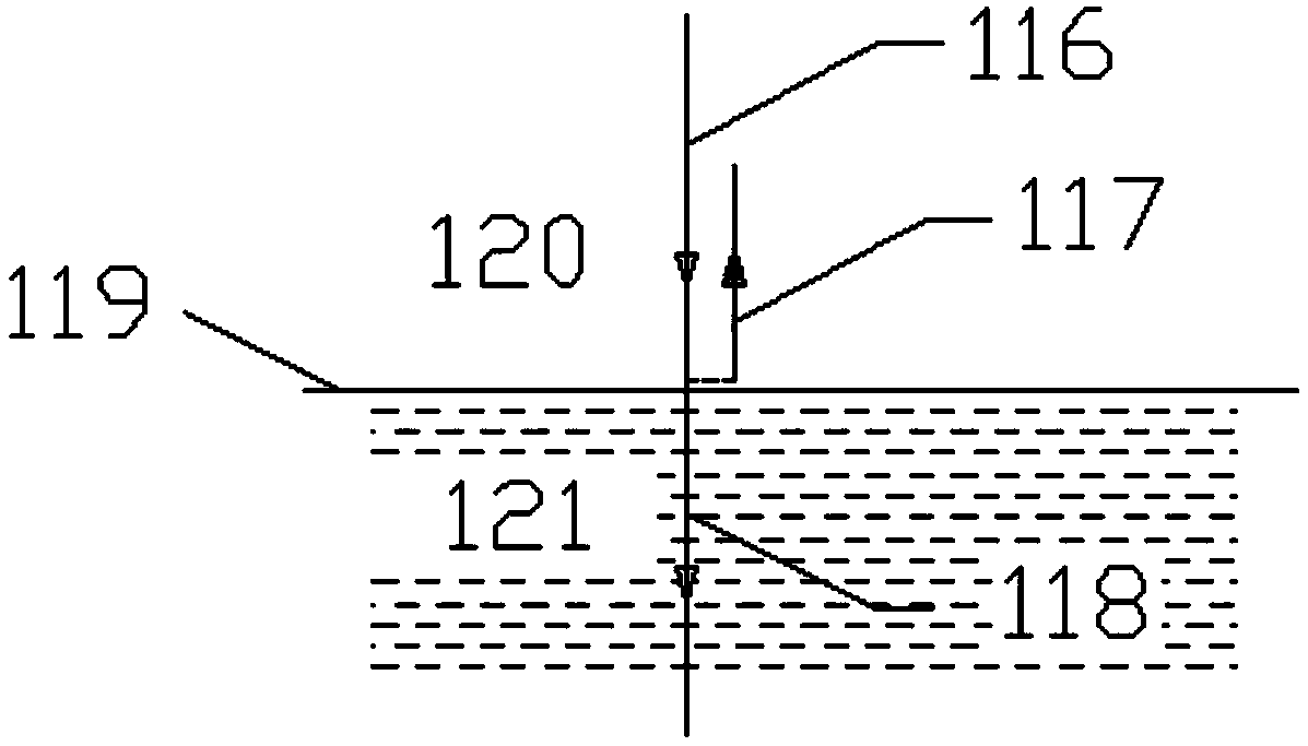
[0038] According to the Fresnel principle, such as figure 1 As shown, the reflectivity R of the interface 119 when the incident light 116 is incident perpendicularly can be calculated by the following formula:

[0039] R = ( n a - n b n a + n b ) 2

[0040] Where: n a Is the refractive index of the medium 120 on the interface 119, n b It is the refractive index of the medium 121 on the lower side of the interface 119. In order to make it easier to distinguish the reflected light from the transmitted light, each light in the figure is drawn separately in the schematic diagram. In practice, all the light travels back and forth on the same straight line. From the above formula, when n a ≈n b When, R≈0, that is, the reflected light 116 almost disappears at this time. The transmittance R of the transmitted light 118 ...


PUM


Abstract

The invention relates to a device and method used for detecting surface shape errors of a plate optical element. The device comprises an optical element support, matching liquid and a matching liquid containing tank. When a vertical interferometer is used for measuring the plate optical element, the device can eliminate interference caused by reflective light of a rear optical surface of the plate optical element on surface shape error detection of the front optical surface, so that reliable optical surface shape error distribution of the optical surface is detected. By means of the device and method, the problem that a common vertical interferometer can not detect the surface shape errors of the plate optical element can be effectively solved, the device and method are simple in principle, manufacturing and use cost is low, and detection of the surface shape errors of the plate optical element can be finished on the condition that an original vertical interferometer structure is not changed. The surface shape errors of the optical element are detected in a non-contact mode, the optical element is not damaged, clamping stress does not exist, the optical element can be cleaned with tap water during the detection process of the surface shape errors of the optical element, and special cleaning solvents and methods are not needed.

Description

technical field [0001] The invention relates to the technical field of optical element detection, in particular to a device and method for detecting surface error of flat optical elements. Background technique [0002] The surface error of optical components is generally measured by interferometer by interferometry. However, in the detection of high-precision flat optical components, the front and rear optical surfaces will reflect light, and the reflected light can be reflected back along the original path, which can interfere with the reference wavefront and form interference fringes on the image detector, that is The reflected light from the rear optical surface interferes with the detection of the front optical surface, making it impossible to effectively detect the surface error of the front optical surface. Taking typical optical glass with a refractive index of n=1.55 as an example, in an atmospheric environment, after calculation, when the light is vertically incide...

Claims


Application Information

Patent Timeline
IPC IPC(8): G01B11/24
Inventor 李云贾辛徐富超邢廷文
Owner INST OF OPTICS & ELECTRONICS - CHINESE ACAD OF SCI
Why Eureka
Try Eureka