Array substrate and liquid crystal display panel

An array substrate and substrate technology, applied in nonlinear optics, instruments, optics, etc., can solve problems such as the open circuit between the common main line 310 and the common line 320, the influence of the quality of the liquid crystal display panel, and the abnormal display, so as to avoid short-circuit phenomenon, reduce Process requirements, the effect of avoiding open circuit phenomenon

Active Publication Date: 2014-06-04
SHENZHEN CHINA STAR OPTOELECTRONICS TECH CO LTD
View PDF5 Cites 6 Cited by
  • Summary
  • Abstract
  • Description
  • Claims
  • Application Information

AI Technical Summary

Problems solved by technology

However, during the panel manufacturing process, it is inevitable that dust will be introduced
The introduction of fine dust can easily cause electrostatic discharge (ESD) phenomenon at the intersection of the common main line 310 and the scanning line 10 and at the via connection between the common main line 310 and the common line 320
At the same time, processes such as deposition, photolithography, etching, stripping, and cleaning will cause ESD phenomena to occur
In this way, it will cause the common main line 310 and the scanning line 10 to be electrically connected at the intersection or cause the common main line 310 and the common line 320 to be disconnected at the connection, thereby causing abnormal display and affecting the quality of the liquid crystal display panel.

Method used


Image

  • Array substrate and liquid crystal display panel
  • Array substrate and liquid crystal display panel
  • Array substrate and liquid crystal display panel

Examples


Embodiment Construction

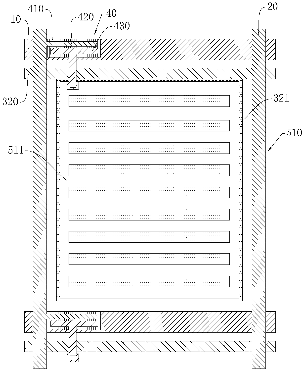
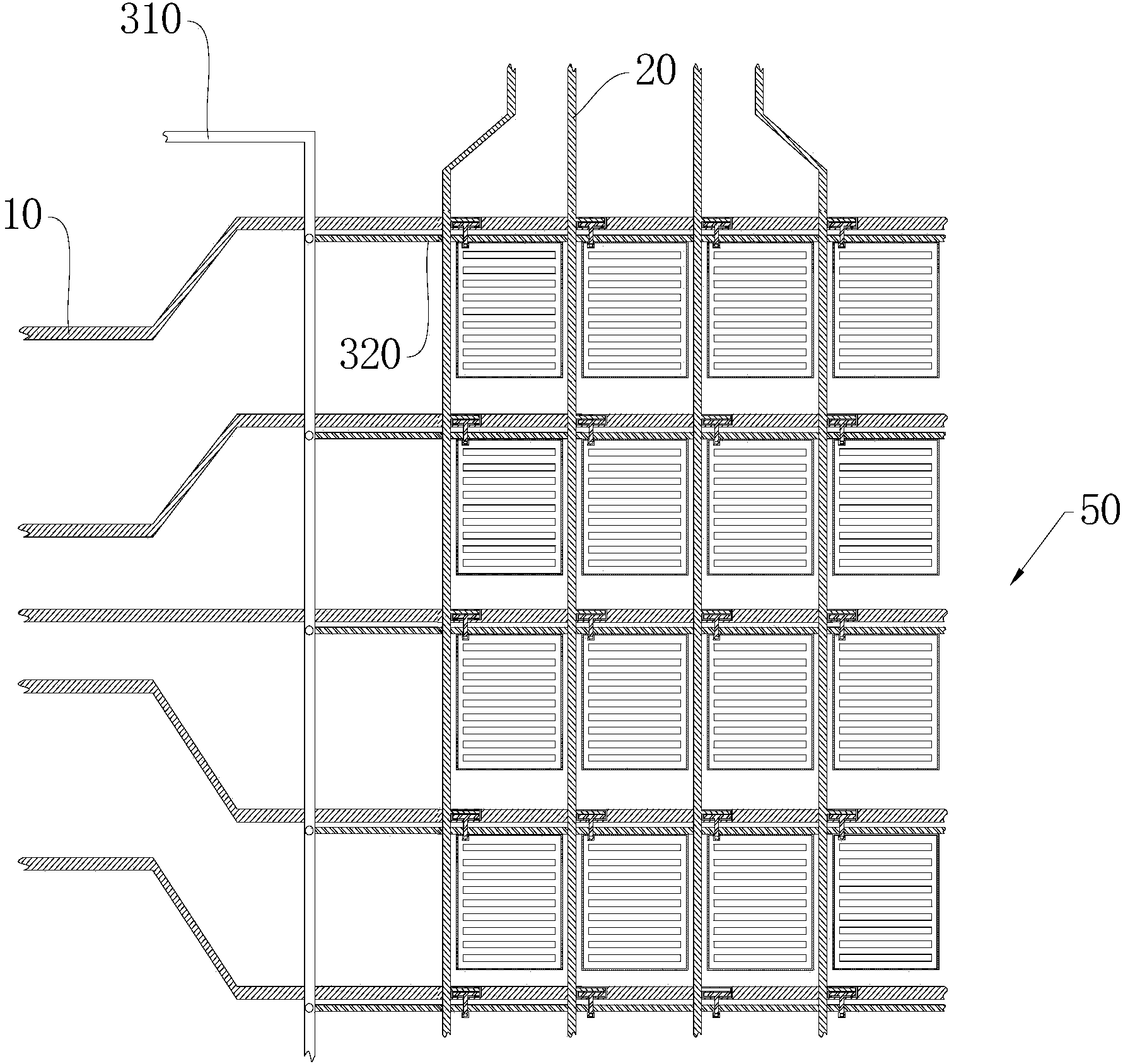
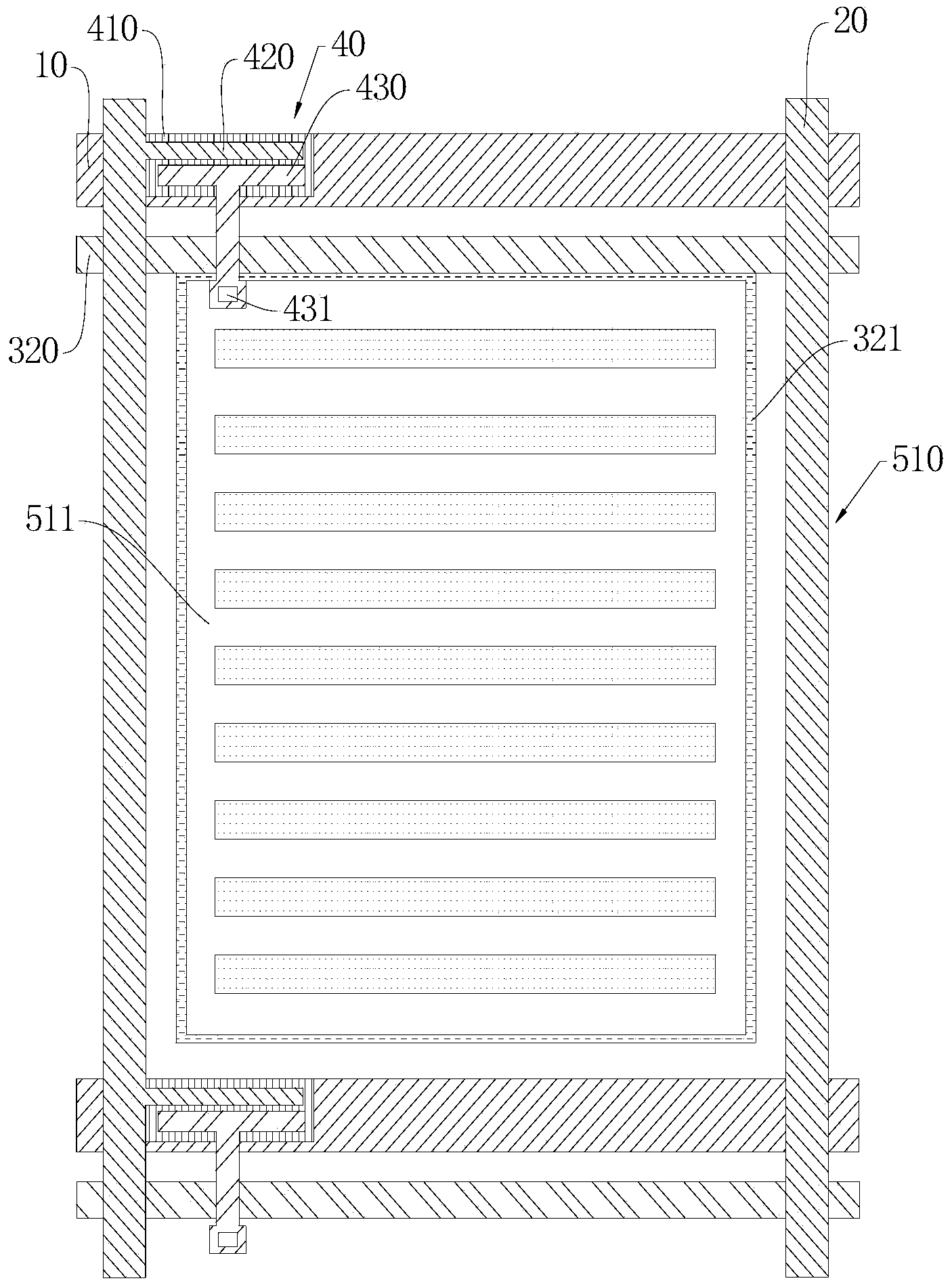
[0025] As mentioned above, the object of the present invention is to provide an array substrate that can effectively prevent the occurrence of ESD and a liquid crystal display panel comprising the array substrate, including: a plurality of scanning lines; a plurality of data lines interlaced with the scanning lines A plurality of pixel units are formed; a plurality of common lines are interspersed in the middle of the scanning lines in parallel, and are interlaced with the data lines, and each common line is connected to a common main line outside the pixel area formed by the pixel unit; the common main line , set on both sides of the pixel area opposite to the scan lines extending to the periphery of the pixel area.

[0026] In order to better illustrate the technical characteristics and structure of the present invention, the following is a detailed description in conjunction with preferred embodiments of the present invention and accompanying drawings.

[0027] refer to i...


PUM


Abstract

The invention provides an array substrate comprising a plurality of scanning lines, a plurality of data lines, a plurality of pixel units crossing with the scanning lines, a plurality of public lines, and a main public line. The public lines penetrate the scanning lines and cross with the data lines, and every public line is connected to the main public line arranged outside a pixel area formed by the pixel units; the main public line and the scanning lines extending to the periphery of the pixel area are correspondingly arranged on two sides of the pixel area. Meanwhile, the invention further provides a liquid crystal display panel with the array substrate. By means of the main public line arranged corresponding to the scanning lines extending to the periphery of the pixel area, crossing between the main public line and the scanning lines can be avoided, and short circuit between the main public line and the scanning lines caused by ESD breakdown can be avoided; meanwhile, the main public line and the public lines can be arranged in one plane, so that breaking of the main public line and public lines can be avoided.

Description

technical field [0001] The invention relates to the technical field of liquid crystal display, in particular to an array substrate and a liquid crystal display panel including the array substrate. Background technique [0002] Nowadays, with the vigorous development of science and technology, the types of information products are introduced to meet the different needs of the public. Most of the early monitors were Cathode Ray Tube (CRT) monitors. Due to their bulky size and high power consumption, the radiation produced was harmful to the health of users who used the monitors for a long time. Therefore, the monitors on the market today are gradually replaced by liquid crystal displays (Liquid Crystal Display, LCD) for the old CRT monitors. [0003] A liquid crystal display (LCD, Liquid Crystal Display) has many advantages such as a thin body, power saving, and no radiation, and thus has been widely used. Most of the liquid crystal display devices currently on the market ar...

Claims


Application Information

Patent Timeline
Patent Type & Authority Applications(China)
IPC IPC(8): G02F1/1362G02F1/1343
CPCG02F1/136286G02F1/136204
Inventor 高冬子
Owner SHENZHEN CHINA STAR OPTOELECTRONICS TECH CO LTD
Why Eureka
Try Eureka