Semiconductor structure and forming method thereof

A technology of semiconductor and ring structure, which is applied in the direction of semiconductor devices, semiconductor/solid-state device manufacturing, semiconductor/solid-state device components, etc., can solve the problems of high cost and low efficiency of chip manufacturing process, and achieve process cost saving, process step saving, The effect of improving process efficiency

Active Publication Date: 2014-06-04
SHANGHAI HUAHONG GRACE SEMICON MFG CORP
View PDF8 Cites 3 Cited by
  • Summary
  • Abstract
  • Description
  • Claims
  • Application Information

AI Technical Summary

Problems solved by technology

[0005] The problem solved by the invention is that in the prior art, the method of fixing and supporting the thinned wafer makes the entire chip manufacturing process inefficient and high in cost

Method used


Image

  • Semiconductor structure and forming method thereof
  • Semiconductor structure and forming method thereof
  • Semiconductor structure and forming method thereof

Examples


Embodiment Construction

[0039] After discovery and analysis, in the prior art, the method of fixing and supporting the thinned wafer makes the entire chip manufacturing process inefficient and the reasons for the high cost are as follows:

[0040] In the prior art, there are mainly two methods for fixing and supporting the wafer during the chip manufacturing process.

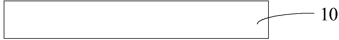
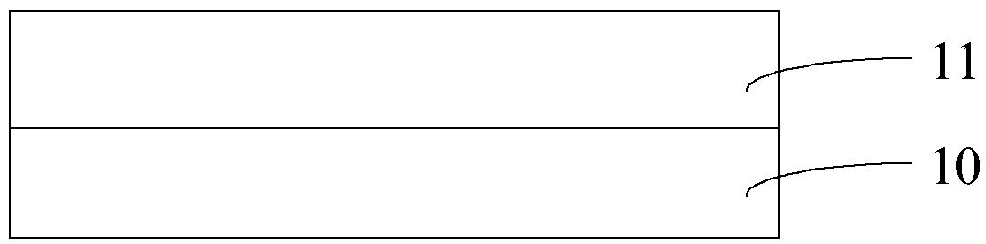
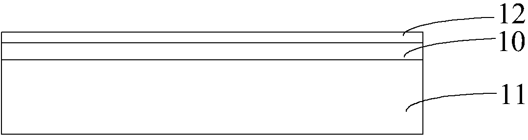
[0041] refer to Figure 1 to Figure 4 , the first method is the glass sheet fixed support method, specifically: refer to figure 1 , providing a wafer 10 with a thickness of 725 microns, on which semiconductor devices (not shown) have been formed, for example, several Insulated Gate Bipolar Transistors (IGBT, Insulated Gate Bipolar Transistor) with a working voltage of 600 volts are formed. ). refer to figure 2 , paste a glass sheet 11 with a thickness of 725-1000 microns on the front surface of the wafer 10 . Next, the wafer 10 is turned over, and the back side of the wafer 10 is thinned by using a chemical mechanical polishing de...


PUM


Abstract

Provided are a semiconductor structure and a forming method thereof. The forming method of the semiconductor structure comprises the steps that a first wafer with a first surface and a second surface opposite to the first surface is provided, the first surface is provided with at least one semiconductor device, and the top of the semiconductor device is a first conducting layer; a second wafer with a third surface and a fourth surface opposite to the third surface is provided, the third surface of the second wafer is provided with at least one imaging second conducting layer, and the second conducting layer and the first conducting layer correspond in position; the top of the first conducting layer and the top of the second conducting layer are connected in a bonding mode; after bonding connection, the second surface is thinned, and accordingly the thickness of the first wafer is the largest all the time; from the fourth surface, a conducting plug is formed in the second wafer, and the bottom of the conducting plug is electrically connected with the second conducting layer; and a third conducting layer is formed on the second surface of the thinned first wafer. According to the method, whole chip manufacturing process efficiency can be improved, and cost is lowered.

Description

technical field [0001] The invention relates to the field of semiconductors, in particular to a semiconductor structure and a forming method thereof. Background technique [0002] With the continuous development of semiconductor technology, in order to continuously reduce the resistance value of the wafer itself, the thickness of the wafer needs to be continuously reduced. Moreover, the thickness of the wafers used to fabricate IGBTs is smaller than that of other semiconductor devices. [0003] After the IGBTs are formed on the wafer, the wafer needs to be thinned to a final thickness of less than 60 microns, and then the wafer is diced to form dies containing the IGBTs, The die is then packaged to form a chip. In the manufacturing process of the above chip, it is necessary to fix and support the thinned wafer. Otherwise, the wafer will be bent due to too small thickness, so that the mechanical arm cannot accurately find the position of the wafer and collide with the wafe...

Claims


Application Information

Patent Timeline
Patent Type & Authority Applications(China)
IPC IPC(8): H01L21/02H01L21/768H01L23/48
CPCH01L21/02016H01L21/76898H01L23/481H01L24/83H01L2221/1068H01L2224/26
Inventor 黄锦才刘玮荪
Owner SHANGHAI HUAHONG GRACE SEMICON MFG CORP
Why Eureka
Try Eureka