Multi-color solder mask layer

A technology of solder mask and color, applied in the direction of coating non-metallic protective layer, secondary treatment of printed circuit, printed circuit components, etc., can solve the problems of long processing time, single printing color, poor bonding force, etc., to achieve cost reduction effect

Inactive Publication Date: 2014-06-18
晏石英
View PDF0 Cites 7 Cited by
  • Summary
  • Abstract
  • Description
  • Claims
  • Application Information

AI Technical Summary

Problems solved by technology

The required processing time is long and the printed color is single
The bonding force between the character layer and the solder mask layer is not good, and the characters are easy to fall off from the solder mask layer

Method used


Image

  • Multi-color solder mask layer
  • Multi-color solder mask layer
  • Multi-color solder mask layer

Examples


Embodiment Construction

[0029] The present invention will be described in further detail below in conjunction with the accompanying drawings and specific embodiments.

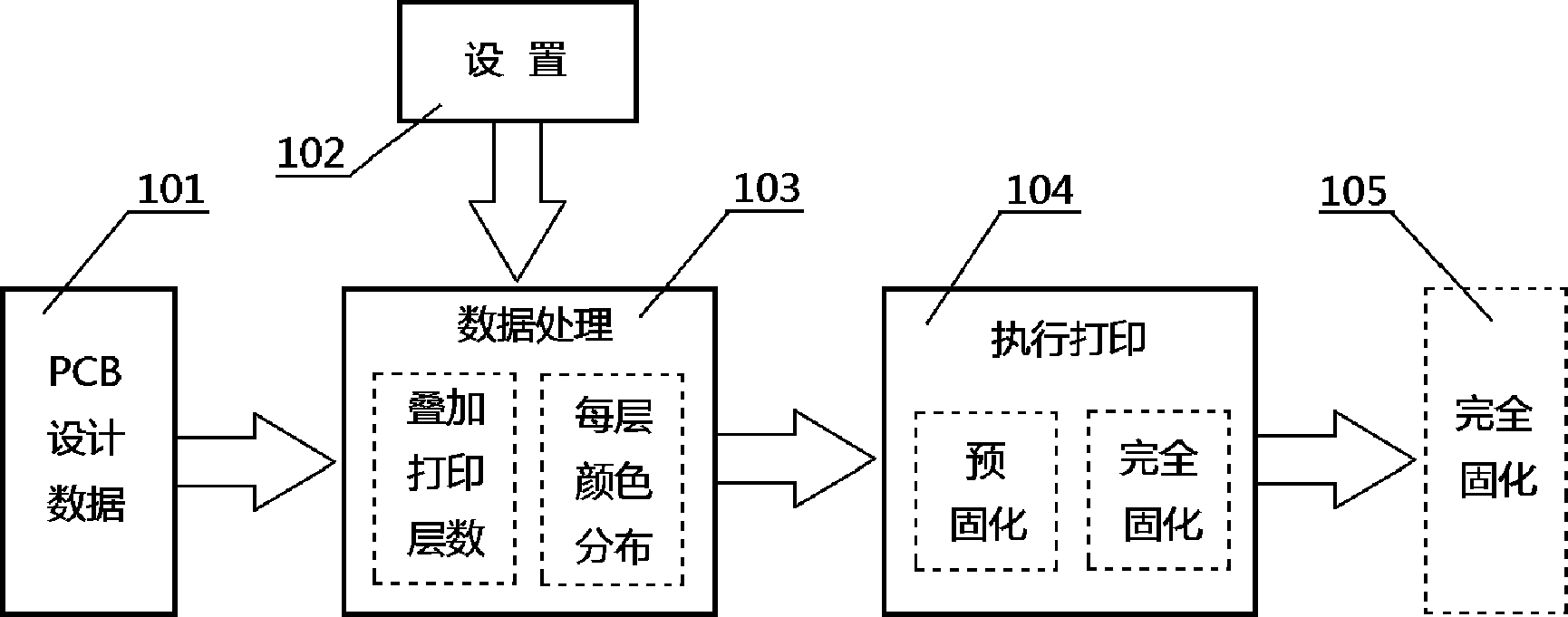
[0030] See attached figure 1 method shown. First, block 103 performs data processing according to the PCB design data represented by block 101 and the settings represented by block 102, and outputs the result. Block 103 processes the data to obtain the data required for printing the solder resist layer, such as: the number of overprinted layers, the color distribution of each layer, and the like.

[0031] Then, block 104 executes the printing task according to the output result of block 103, and prints out the required solder resist layer.

[0032] Because the ink used to print the solder mask is different, different methods are required for curing. UV solder mask ink is selected, which needs to be cured by UV light, and can be pre-cured first and then fully cured, or directly fully cured.

[0033] As a commonly used curing proces...


PUM


Abstract

The invention discloses a multi-color solder mask layer. Different colors of the solder mask layer can be used for distinguishing a functional area or a special area. According to the solder mask layer, one or more colors different from the background color are used for being displayed as characters, and accordingly the character printing procedure is omitted.

Description

technical field [0001] The invention relates to a solder resist layer and characters of a PCB (printed circuit board, including a flexible circuit board and a hard circuit board), and a printing method thereof. technical background [0002] At present, PCB is first printed with solder mask (also known as solder mask, soldering protective layer), and then printed with characters (also known as text, word mark, character mark). The traditional printing method is mainly based on silk screen printing. With the rise of inkjet printing technology, solder mask printing equipment and character printing equipment have appeared. [0003] According to the existing technology and process, the solder mask and characters on both sides of the PCB are printed separately, and different colors can be printed on both sides. But the solder mask or characters on the same side can only be printed in one color, and the solder mask printing and character printing are printed as two processes. The...

Claims


Application Information

Patent Timeline
Patent Type & Authority Applications(China)
IPC IPC(8): H05K1/02H05K3/28
Inventor 晏石英
Owner 晏石英
Why Eureka
Try Eureka