Pixel unit structure, array substrate structure and liquid crystal display device

A technology of liquid crystal display device and pixel unit, which is applied in nonlinear optics, instruments, optics, etc., and can solve problems such as reducing the effect of display

Active Publication Date: 2014-07-09
XIAMEN TIANMA MICRO ELECTRONICS +1
View PDF3 Cites 10 Cited by
  • Summary
  • Abstract
  • Description
  • Claims
  • Application Information

AI Technical Summary

Problems solved by technology

There is a black area 11 on the side of the pixel unit away from the TFT 12, and

Method used


Image

  • Pixel unit structure, array substrate structure and liquid crystal display device
  • Pixel unit structure, array substrate structure and liquid crystal display device
  • Pixel unit structure, array substrate structure and liquid crystal display device

Examples


Embodiment 1

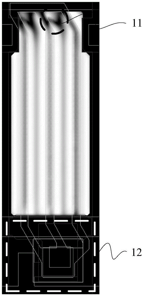
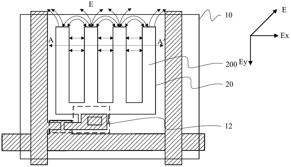
[0039] Please refer to image 3 , is a schematic top view structural diagram of the pixel unit provided by Embodiment 1 of the present invention. As shown in the figure, the pixel unit provided by Embodiment 1 includes: a data line 210, a scan line 220, a TFT 12, a first electrode 40, a second electrode 50, and a shielding electrode 60, and the first electrode 40 and the second electrode 50 form Infield.

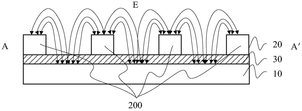
[0040] Specifically, the first electrode 40 is a planar electrode, the second electrode 50 includes a plurality of strip electrodes 500 , and a first insulating layer (not shown) for insulation is between the first electrode 40 and the second electrode 50 . In the first embodiment, the second electrode 50 is a pixel electrode, and the first electrode 40 is a common electrode. The plurality of strip electrodes 500 of the second electrode 50 are arranged at intervals, one end of the plurality of strip electrodes 500 of the second electrode 50 is connected to the drain of the...

Embodiment 2

[0046] Please refer to Figure 7 , is a schematic top view structure diagram of the pixel unit provided by Embodiment 2 of the present invention. As shown in the figure, the pixel unit provided in Embodiment 2 includes: data line 210, scan line 220, TFT 12, first electrode 40, second electrode 50, shielding electrode 60, the first electrode 40 and the second electrode 50 form an in-plane field.

[0047] Specifically, the first electrode 40 is a planar electrode, the second electrode 50 includes a plurality of strip electrodes 500 and connecting electrodes 510, and a first insulating layer that plays an insulating role is also included between the first electrode 40 and the second electrode 50 (not shown). The plurality of strip electrodes 500 of the second electrode 50 are arranged at intervals. In the second embodiment, the second electrode 50 is a pixel electrode, and the first electrode 40 is a common electrode. One end of the plurality of strip electrodes 500 of the se...

Embodiment 3

[0055] Please refer to Figure 13 , is a schematic diagram of an array structure composed of a plurality of pixel units provided in Embodiment 3 of the present invention. As shown in the figure, the array structure provided by Embodiment 3 includes a plurality of data lines 210 , a plurality of scan lines 220 , and a plurality of pixel units 1 defined by intersections of the plurality of data lines 210 and the plurality of scan lines 220 .

[0056] Specifically, each pixel unit 1 includes a first electrode 40 , a second electrode 50 and a shielding electrode 60 , and an in-plane field is formed between the first electrode 40 and the second electrode 50 . The first electrode 40 is a planar electrode, the second electrode 50 includes a plurality of strip electrodes 500 , and a first insulating layer (not shown) for insulation is between the first electrode 40 and the second electrode 50 . The plurality of strip electrodes 500 of the second electrode 50 are arranged at intervals...


PUM


Abstract

The invention discloses a pixel unit structure, an array structure and a liquid crystal display device to solve the problem of poor display effect of a liquid crystal display device in the prior art. The pixel unit structure comprises a first electrode, a second electrode and shielding electrodes, the first electrode is of a faceted structure, a first insulating layer is formed on the first electrode, the second electrode is formed on the first insulating layer and comprises a plurality of strip electrodes which are arranged at intervals, and the shielding electrodes are arranged at the tail ends of the strip electrodes of the second electrode. By the aid of the technical scheme, when the pixel unit structure has electric signals, an Ey-direction electric field generated at the tail ends of the strip electrodes of the second electrode is shielded owing to the shielding electrodes, so that domain lines are effectively avoided, display molecules corresponding to all display areas of the pixel unit structure can rotate according to a preset mode, and image display effects are improved.

Description

technical field [0001] The invention relates to the field of display device manufacturing, in particular to a pixel unit structure, an array structure and a liquid crystal display device. Background technique [0002] With the rapid development of science and technology, the performance of display devices of electronic products has been greatly improved, and various large-size, high-resolution display devices have been widely used. [0003] Currently, display devices generally adopt TN (Twisted Nematic, twisted nematic) display mode, ADS (ADvanced Super Dimension Switch, advanced super dimension field switching technology) display mode and FFS (Fringe Filed Switching; fringe field switching technology) display mode. [0004] The FFS display mode is favored by the market due to its advantages such as large viewing angle and high light transmittance. However, in the FFS display mode in the prior art, display abnormalities may occur on the side of the pixel unit away from the ...

Claims


Application Information

Patent Timeline
IPC IPC(8): G02F1/1343G02F1/1333
Inventor 张沼栋沈柏平宋琼
Owner XIAMEN TIANMA MICRO ELECTRONICS
Why Eureka
Try Eureka