Photomask detection method

A detection method and mask technology, applied in optics, originals for photomechanical processing, instruments, etc., can solve the problem that scanning equipment cannot fully detect defects, and achieve the effect of eliminating blind spots in detection

Inactive Publication Date: 2014-07-09
SHANGHAI HUALI MICROELECTRONICS CORP
View PDF3 Cites 6 Cited by
  • Summary
  • Abstract
  • Description
  • Claims
  • Application Information

AI Technical Summary

Problems solved by technology

[0009] The purpose of the present invention is to provide a photomask inspection method to solve the problem that the scanning equipment in the prior art cannot fully detect defects during photomask inspection

Method used


Image

  • Photomask detection method
  • Photomask detection method
  • Photomask detection method

Examples


Embodiment Construction

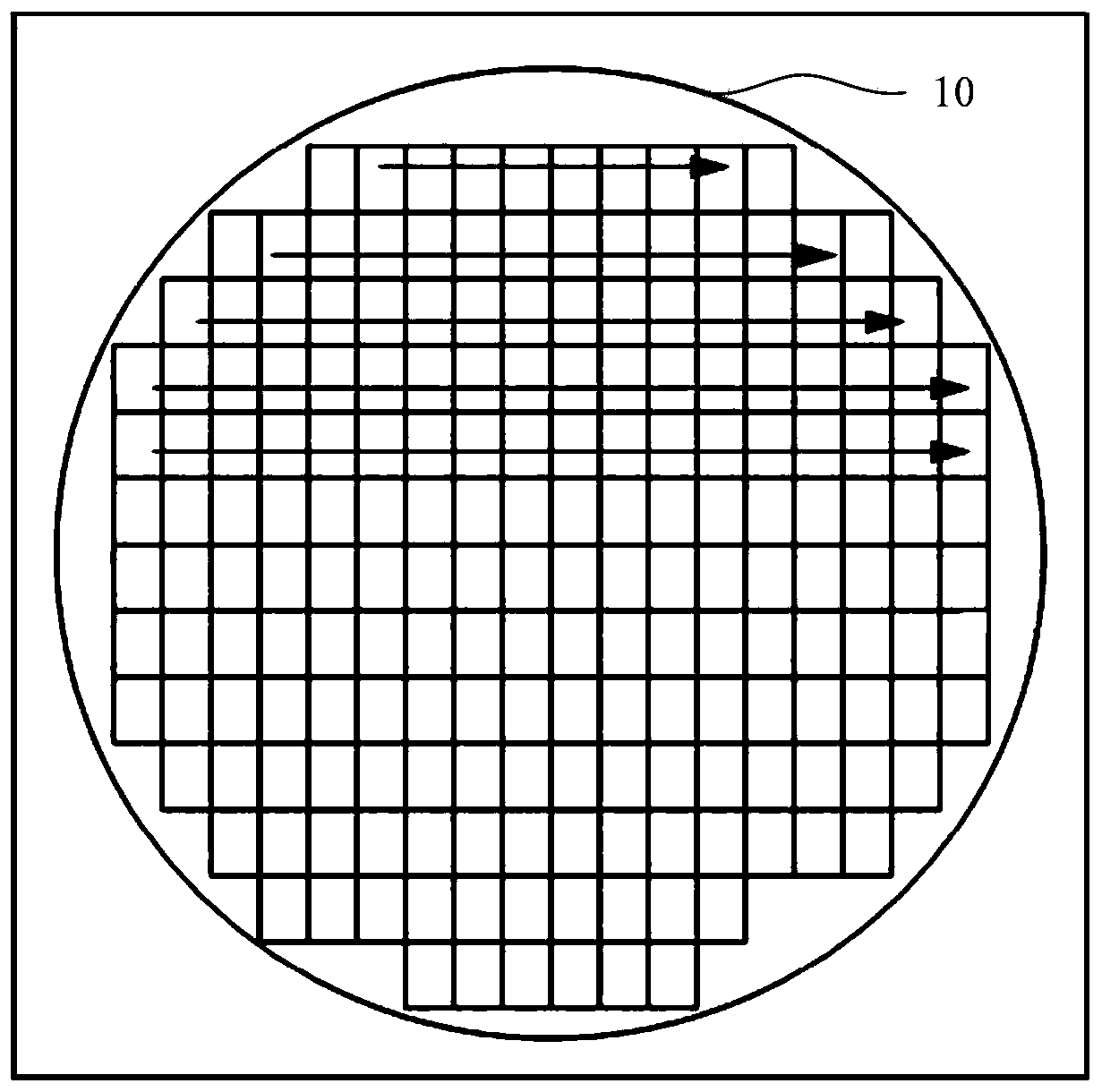
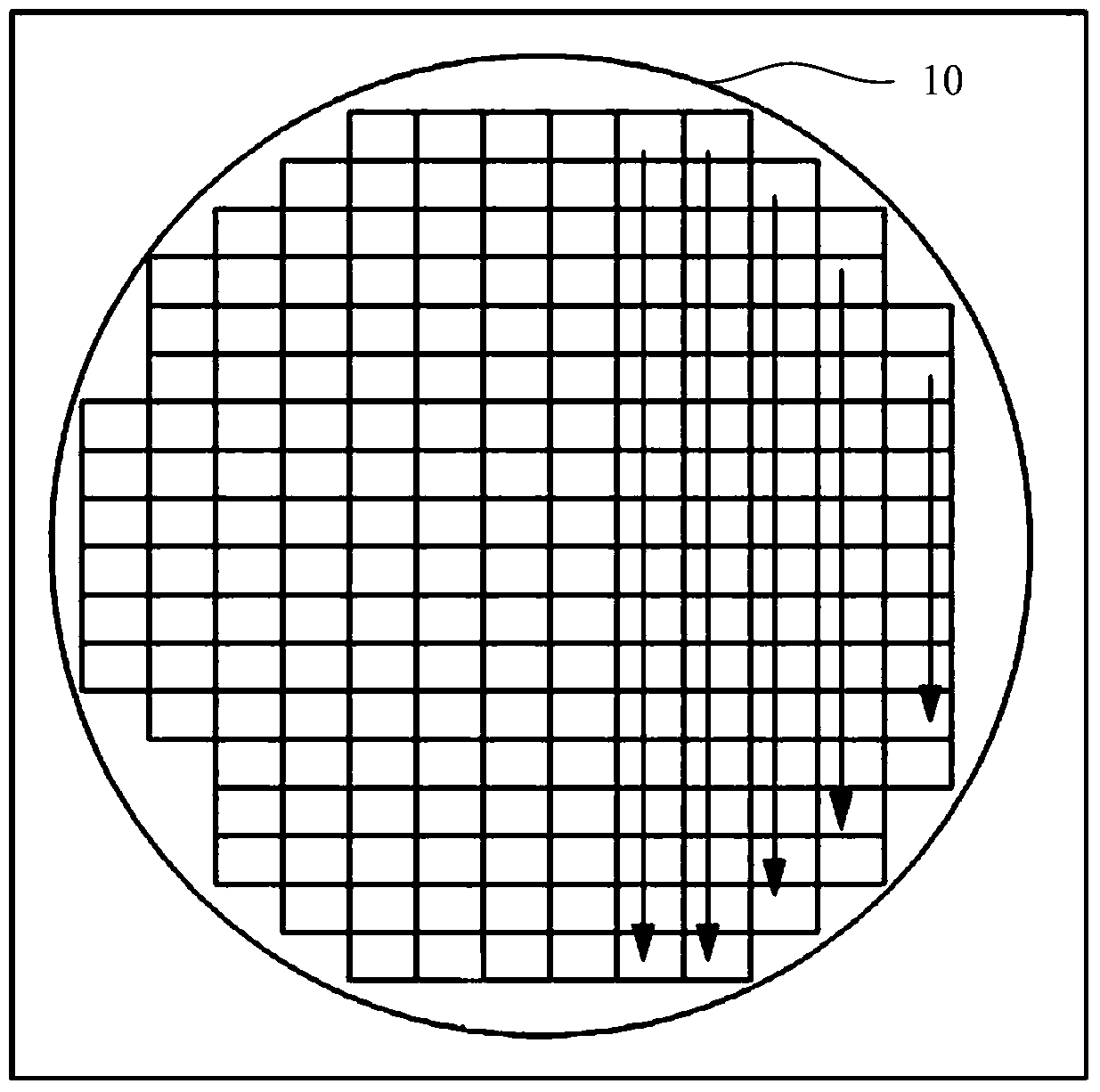
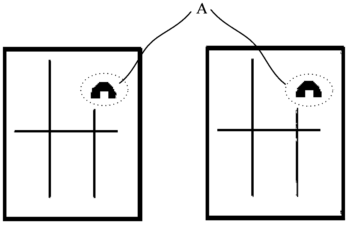
[0026] The photomask inspection method proposed by the present invention will be described in further detail below in conjunction with the accompanying drawings and specific embodiments. Advantages and features of the present invention will be apparent from the following description and claims. It should be noted that all the drawings are in a very simplified form and use imprecise scales, and are only used to facilitate and clearly assist the purpose of illustrating the embodiments of the present invention.

[0027] Existing scanning equipment cannot fully detect defects during mask inspection, resulting in defective products. The inventor conducted in-depth research on this, and found that the reason why the existing scanning equipment cannot fully detect defects during mask inspection is that the comparison method adopted by the scanning equipment is unique, so the scanning of the control sheet in actual production The program can only use one comparison method, that is, t...


PUM


Abstract

The invention provides a photomask detection method. The photomask detection method comprises the following steps: providing a control wafer, and transferring the patterns of the photomask to be detected to the control wafer; performing primary defect scanning on the control wafer; rotating the control wafer at 90 degrees, and then performing secondary defect scanning. According to the photomask detection method provided by the invention, the patterns of the photomask to be detected are transferred to the control wafer, and the control wafer is scanned in two perpendicular directions to eliminate detection blind points of scanning equipment, so that defects can be comprehensively defected by the scanning equipment.

Description

technical field [0001] The invention relates to the technical field of semiconductor manufacturing, in particular to a photomask detection method. Background technique [0002] With the rapid development of semiconductor manufacturing technology, in order to achieve faster computing speed, larger data storage capacity and more functions of semiconductor devices, semiconductor chips are developing towards higher integration. The higher the integration level of the semiconductor chip, the smaller the critical dimension (CD) of the semiconductor device, and the more complex the circuit structure of the chip. At present, the feature size of VLSI has entered the range of tens to hundreds of nanometers. [0003] In the manufacturing process of a semiconductor chip, it is usually necessary to carry out multiple photolithography to form various microscopic patterns with precise dimensions on the semiconductor substrate. Among them, a photomask (Photo Mask), also called a photomask...

Claims


Application Information

Patent Timeline
Patent Type & Authority Applications(China)
IPC IPC(8): G03F1/00
Inventor 何理许向辉郭贤权陈超
Owner SHANGHAI HUALI MICROELECTRONICS CORP
Why Eureka
Try Eureka