A method to improve the channel mobility of n-type dimosfet based on n-type nano-thin layer

A mobility, N-type technology, applied in the field of microelectronics, can solve the problems of reduced gate oxide reliability, affected device performance, rough contact interface, etc., to reduce trap charges, increase mobility, and reduce interface roughness. Effect

CN103928344BActive Publication Date: 2017-04-05XIDIAN UNIV
3 Cites 0 Cited by

Patent Information

Authority / Receiving Office
CN · China
Patent Type
Patents(China)
Current Assignee / Owner
Publication Date
2017-04-05

Smart Images

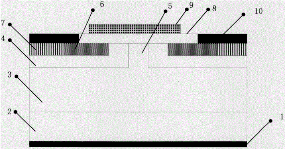
  • Figure 1
    Figure 1
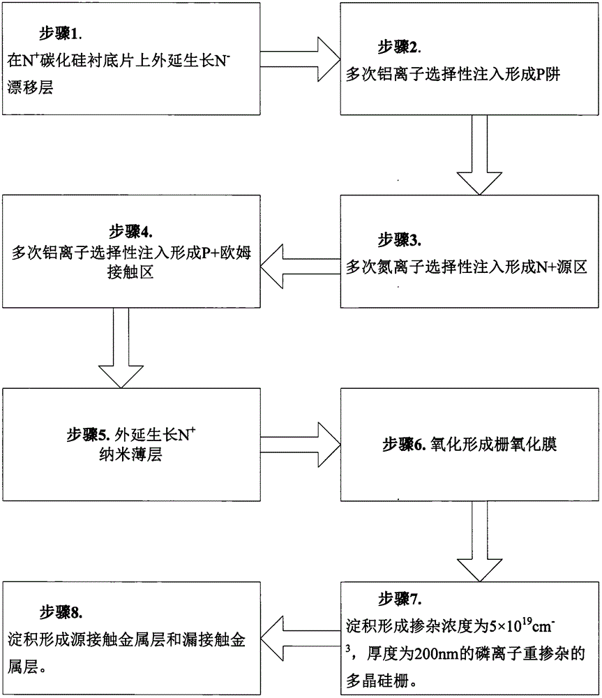
  • Figure 2
    Figure 2
Patent Text Reader

Abstract

The invention discloses a method for improving N-typed DiMOSFET channel mobility based on an N-typed nanometer thin layer, the mode of nitrogen injecting of conducting channel layer through injection forming is changed to the mode of nitrogen injecting of conducting channel layer through an N+ epitaxial layer a formed by extension on the basis of an existing ion injection technology. For an N-channel DiMOSFET device, the extension thickness ranges from 10 nm to 20 nm, the doping concentration ranges from 1*10<18> cm<-3> to 1*10<19>cm<-3>, then oxidation is conducted in a gate oxide technology, nitrogen ions are only contained in a gate oxide layer and a Sic interface, and dangling bonds on the surface are reduced. Compared with existing ion injection nitrogen, the epitaxial layer a is introduced, the problems of rough contact interface of SiC and SiO2, high lattice loss, low activation rate and the like due to the nitrogen injection technology are avoided, and the SiC DiMOSFET device which is high in electronic mobility, low in on-resistance and low in power consumption is obtained.
Need to check novelty before this filing date? Find Prior Art

Description

technical field

[0001] The invention belongs to the technical field of microelectronics and relates to a method for improving channel mobility of an N-type DiMOSFET based on N-type epitaxy. Background technique

[0002] SiC has become one of the most advantageous semiconductor materials for manufacturing high-temperature, high-power electronic devices due to its excellent physical, chemical and electrical properties, and has a power device quality factor much greater than that of Si materials. The research and development of SiC power device MOSFET began in the 1990s. It has a series of advantages such as high input impedance, fast switching speed, high operating frequency, and high temperature and high pressure resistance. It has been used in switching regulated power supplies, high-frequency heating, automotive electronics and power amplifiers. and so on have been widely used.

[0003] However, the current SiC power MOS devices SiC and SiO 2 The poor contact interface qu...

Examples

Embodiment 1

[0036] Step 1. In N + Epitaxial growth of N on SiC substrate - Drift layer.

[0037] to N + The silicon carbide substrate 2 was cleaned by RCA cleaning standard, and then epitaxially grown on the surface of the substrate with a thickness of 8 μm and a nitrogen ion doping concentration of 1×10 15 cm -3 N - Drift layer 3, such as figure 2 In step 1, the process conditions are as follows: the epitaxy temperature is 1570° C., the pressure is 100 mbar, the reaction gas is silane and propane, the carrier gas is pure hydrogen, and the impurity source is liquid nitrogen.

[0038] Step 2. Multiple times of selective implantation of aluminum ions to form a P well.

[0039] (2.1) Deposit a layer of SiO with a thickness of 0.2 μm on the front side of the silicon carbide wafer by low-pressure hot-wall chemical vapor deposition 2 layer, and then deposit Al with a thickness of 1 μm as a barrier layer for the ion implantation of the P well 4, and form the P well implantation region by...