Double-layer wafer transfer cavity

A cavity and double-layer technology, which is applied in the field of double-layer film transfer cavity structure, can solve the problems of complicated maintenance and increase equipment use cost, and achieve the effect of reducing equipment use cost, reasonable structure and easy overall equipment maintenance.

Inactive Publication Date: 2014-07-16
PIOTECH CO LTD
View PDF3 Cites 5 Cited by
  • Summary
  • Abstract
  • Description
  • Claims
  • Application Information

AI Technical Summary

Problems solved by technology

[0003] The purpose of the present invention is to solve the above problems, and mainly solve the problem that the existing technology makes the overall maintenance of the equipment complex and inc

Method used


Image

  • Double-layer wafer transfer cavity

Examples


Embodiment

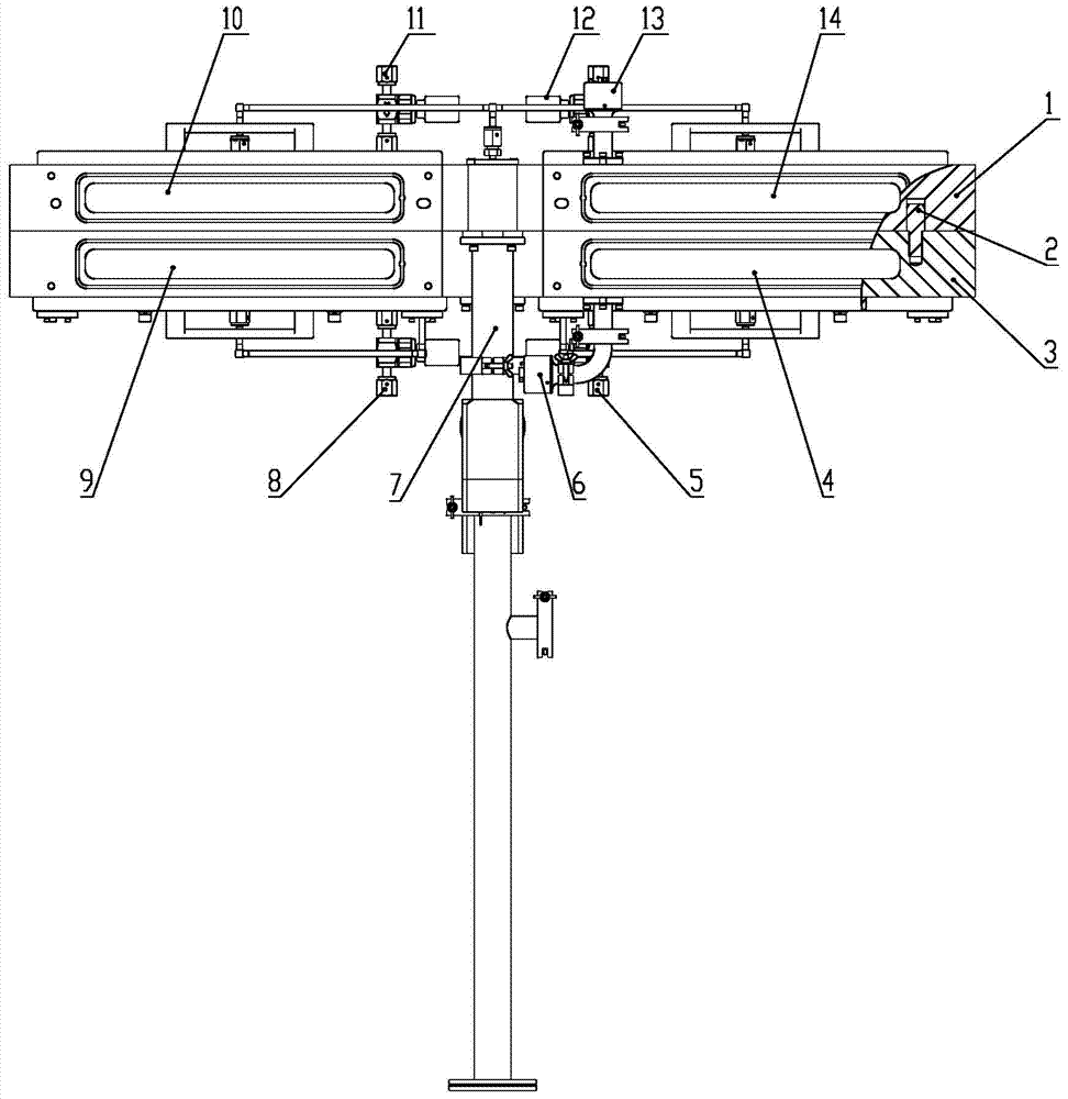
[0012] refer to figure 1 , double-layer film transfer chamber, including upper chamber 1, positioning pin 2, lower chamber 3, chamber A4, chamber B9, chamber C10 and chamber D14, exhaust pipeline 7, vacuum measurement component A6 and vacuum Measuring component B13 and valve body A5, valve body B8, valve body C11 and valve body D12 of balanced atmosphere. The above-mentioned double-layer film transfer cavity is composed of an upper layer cavity 1 and a lower layer cavity 3 , and is fixed by pins 2 . The double-layer chambers have independent pumping pipelines 7, vacuum measurement components A6 and vacuum measurement components B13. The upper and lower chambers can independently complete the film transfer function, and can be used for both single-layer film transfer and double-layer film transfer.

[0013] The above cavities all have two interconnected chambers, the upper chamber 1 is composed of chamber C10 and chamber D14; the lower chamber 3 is composed of chamber A4 and c...


PUM


Abstract

Disclosed is a double-layer wafer transfer cavity. The double-layer wafer transfer cavity mainly solves the problem that whole device maintenance is complex and the device using cost is increased so as to achieve the function of upper-layer wafer transfer and lower-layer wafer transfer in the prior art, and can achieve independent wafer transfer with double-layer multiple cavities. An upper-layer cavity body and a lower-layer cavity body of double-layer multiple cavities are independent closed cavity bodies respectively. The cavity bodies can independently conduct the wafer transfer operation and cannot affect each other. Each cavity body is internally provided with two chambers communicated with each other. Each chamber can conduct independent operations of wafer transfer and wafer taking, and the operations cannot affect each other. The double-layer wafer transfer cavity has the advantages that the structure is reasonable, the whole device maintenance is easier, and the device using cost can be reduced. The double-layer wafer transfer cavity can be widely applied to the technical field of semiconductor film deposition application and preparation.

Description

technical field [0001] The invention relates to a double-layer film transfer chamber structure, especially a chamber that is connected to each other but can be operated independently in each layer of the chamber. This structure is mainly used in semiconductor coating equipment and belongs to the application of semiconductor thin film deposition. and preparation technology. Background technique [0002] Existing semiconductor coating equipment has higher and higher requirements on the functionality and applicability of the chamber. The wafer transfer chamber is an important chamber for wafer transfer in and out. The transfer chamber must not only be suitable for different equipment requirements, At the same time, there must be a chamber that is relatively independent and has the function of transferring the film. At present, most of the existing film transfer chambers are single-layer chambers, and there are also brackets of unequal heights placed in the single-layer chamber...

Claims


Application Information

Patent Timeline
IPC IPC(8): H01L21/677C23C16/44
CPCH01L21/67178H01L21/67126H01L21/6719H01L21/67196C23C16/44
Inventor 吴凤丽姜崴方仕彩
Owner PIOTECH CO LTD
Why Eureka
Try Eureka