Chip and method testing chip

A chip and test signal technology, applied in electronic circuit testing, instruments, electrical digital data processing, etc., can solve problems such as the inability to achieve long-distance transmission

Active Publication Date: 2013-05-15
LONTIUM SEMICON CORP
View PDF4 Cites 1 Cited by
  • Summary
  • Abstract
  • Description
  • Claims
  • Application Information

AI Technical Summary

Problems solved by technology

However, when using a USB cable to transmit a USB signal, it can only transmit

Method used


Image

  • Chip and method testing chip
  • Chip and method testing chip
  • Chip and method testing chip

Examples


Embodiment 1

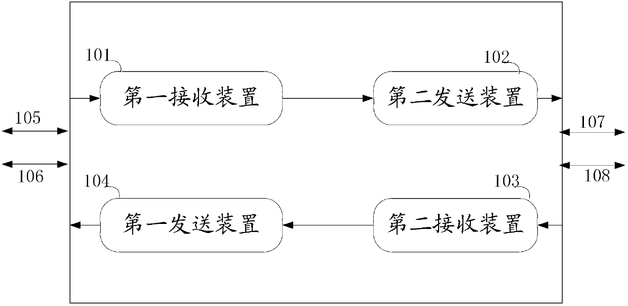
[0092] Embodiment 1 of the present invention provides a specific structure of a chip that can realize the transfer function, and its structural schematic diagram is as follows figure 1 Shown:

[0093] In this embodiment, the first receiving device 101 may be a USB full-speed or low-speed receiving device, capable of receiving full-speed or low-speed USB signals from the outside of the chip through the first pin 105 and the second pin 106 on the chip, that is, complying with USB1. 1 Protocol full speed (12Mb / s) or low speed (1.5Mb / s) USB signal;

[0094]The second sending device 102 can be a full-speed or low-speed sending device at the network cable interface end, capable of receiving a full-speed or low-speed USB signal sent by a USB full-speed or low-speed receiving device, and performing format conversion on the USB signal (for example, it can be converted into a full-speed or low-speed network cable signal) , and send the signal after the format conversion to the outside ...

Embodiment 2

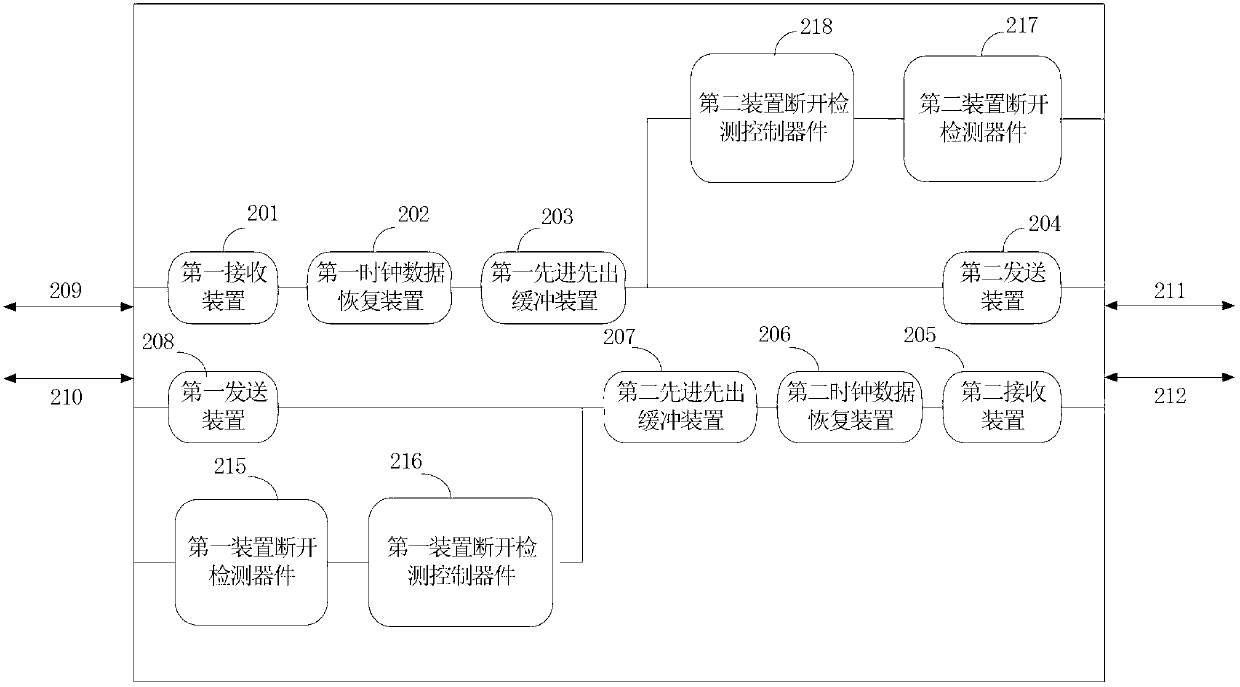
[0100] figure 2 It shows a schematic structural diagram of a chip capable of realizing the switching function provided by Embodiment 2 of the present invention, and the chip includes:

[0101] The first receiving device 201 is configured to receive a first signal and send the first signal to a first high-speed clock data recovery device 202;

[0102] Specifically, the first signal can be received from outside the chip through the first pin 209 and the second pin 210 on the chip; the first receiving device 201 can be a different type of receiving device, for example, it can be used to receive USB signals The receiving device can also be a receiving device for receiving network cable signals or other types of signals. Correspondingly, the first signal can be a signal conforming to the USB2.0 protocol, or a signal conforming to the network cable protocol, etc., and the first signal The signal can be a high-speed signal, that is, its frequency is not less than 480 / 7Mbit / s, for e...

Embodiment 3

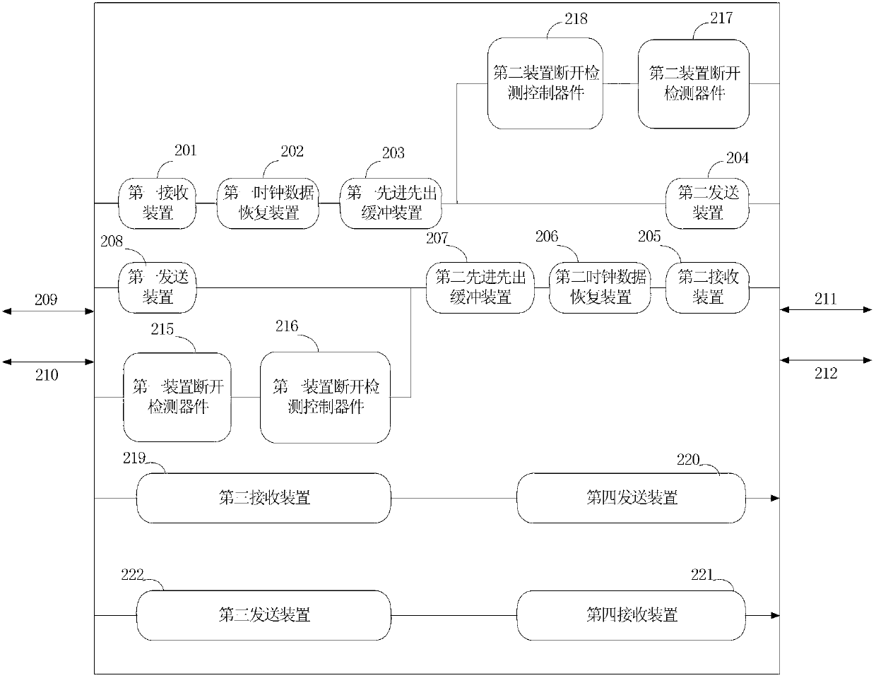
[0122] image 3 A schematic structural diagram of a chip according to Embodiment 3 of the present invention is shown, wherein the chip includes the structures in Embodiment 1 and Embodiment 2 above, namely image 3 The chip in the figure 2 The structure obtained after adding the third receiving means 219, the fourth sending means 220, the fourth receiving means 221 and the third sending means 222 on the basis of the above;

[0123] Wherein, the third receiving device 219 may be a USB full-speed or low-speed receiving device, capable of receiving full-speed or low-speed USB signals from outside the chip through the first pin 209 and the second pin 210 on the chip;

[0124] The fourth sending device 220 can be a full-speed or low-speed sending device at the network cable interface end, capable of receiving a full-speed or low-speed USB signal sent by a USB full-speed or low-speed receiving device, and performing format conversion on the USB signal (for example, it can be conve...


PUM


Abstract

The invention provides a chip and a method testing the chip. The method testing the chip includes that a first transmitting device receives a first test signal which is sent by a test device, converts the first test signal into a second test signal, and sends the second test signal to the exterior of the chip. A first receiving device receives the second test signal, and forwards the second test signal to a second transmitting device. The second transmitting device receives the second test signal, converts the second test signal to a third test signal, and sends the third test signal to the exterior of the chip. The second receiving device receives a third test signal, and returns to a test device. The test device compares whether the third test signal is consistent with the first test signal, if the third test signal is consistent with the first test signal, the function and performance of the chip are correct. The first test signal, the second test signal and the third test signal form a loop outside the chip, and a test path can be adopted to test whether function and performance of multiple devices are correct or not.

Description

technical field [0001] The invention belongs to the technical field of CMOS integrated circuit design, and in particular relates to a chip with switching function and a method for testing the chip. Background technique [0002] The USB interface is a relatively commonly used interface technology at present, and it is widely used in daily life, such as the connection of U disk, mouse keyboard and PC, USB mobile hard disk, etc. USB interfaces mainly include USB1.1, USB2.0, and USB3.0. Among them, USB1.1 interfaces mainly support low-speed (low speed, 1.5Mb / s) and full-speed (full speed, 12Mb / s) USB signals. Transmission, USB2.0 interface supports high-speed 480Mb / sUSB signal transmission, and USB3.0 supports super-speed 5Gb / sUSB signal transmission. [0003] With the continuous development of USB technology, long-distance transmission of USB signals is required. However, when using a USB cable to transmit a USB signal, it can only transmit a range of 5m, which cannot achieve...

Claims


Application Information

Patent Timeline
IPC IPC(8): G06F13/40G01R31/28
Inventor 边慧付家喜邰连梁胡盛泉任殿升陈峰储超群刘清卫李广仁谢长倩
Owner LONTIUM SEMICON CORP
Why Eureka
Try Eureka