Pixel unit and pixel array thereof
A technology of pixel unit and pixel array, applied in instruments, nonlinear optics, optics, etc., can solve the problems of reducing transmittance, reducing transmittance, etc., so as to improve transmittance, overcome the problem of color shift, and have no color shift. effect of the phenomenon
- Summary
- Abstract
- Description
- Claims
- Application Information
AI Technical Summary
Problems solved by technology
Method used
Image

Examples
no. 1 example
[0021] For the first example, please refer to Figure 1 to Figure 5 .
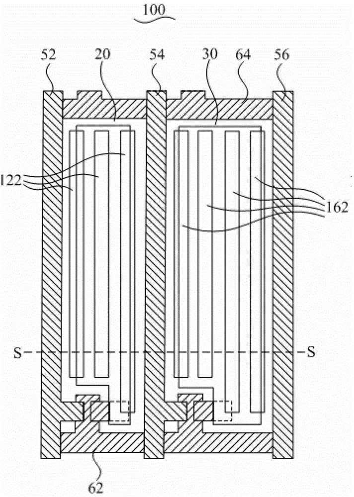
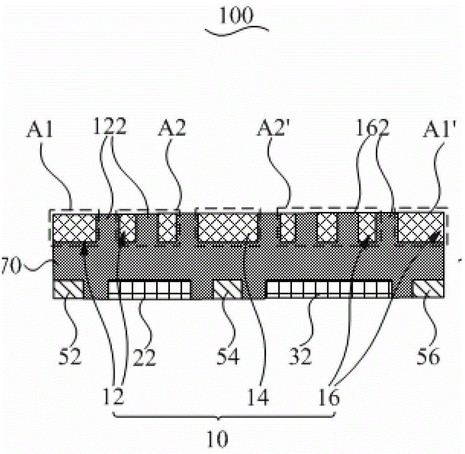
[0022] combine figure 1 and figure 2 As shown, the pixel unit 100 includes a common electrode 10 , a first sub-pixel 20 , a second sub-pixel 30 , a pixel electrode 22 and a pixel electrode 32 .
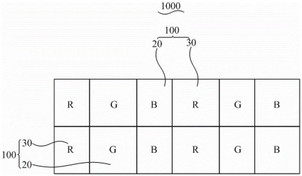
[0023] The three data lines 52, 54 and 56 are arranged in parallel at intervals along the vertical direction. The two scanning lines 62 and 64 are arranged in parallel at intervals along the horizontal direction. The data lines 52 , 54 and 56 criss-cross with the scan lines 62 and 64 , and they enclose two quadrilateral regions, which are respectively defined as the first sub-pixel 20 and the second sub-pixel 30 . The first sub-pixel 20 and the second sub-pixel 30 respectively represent any one of R (red), G (green) and B (blue).
[0024] The pixel electrodes 22 and 32 are respectively located in the first sub-pixel 20 and the second sub-pixel 30 . The pixel electrodes 22 , 32 are located on the same layer ...
no. 2 example
[0032] For the second embodiment, please refer to Figure 5 to Figure 7 .
[0033] The pixel unit 100a in this embodiment includes three sub-pixels: one 30a and two 20a. The structures of the sub-pixels 20a and 30a are the same as those in the first embodiment, and the sub-pixel 20a is also provided with three through-slots 122a, and the sub-pixel 30a is provided with four through-slots 162a. The through grooves 122a, 162a are the same as the through grooves in the first embodiment, and will not be repeated here. In the pixel unit 100a, there are 10 through grooves in total. Compared with the pixel unit using sub-pixels in the prior art, the number of through grooves is increased. However, since the area of each sub-pixel and the number of corresponding slots are different, the light transmission area of each sub-pixel is different. Compared with the pixel unit of the prior art, the sub-pixel transmittance ratio of R, G and B is not within the standard value range Insi...
no. 3 example
[0039] For the third embodiment, please refer to Figure 8 .
[0040] The pixel unit 100b in this embodiment includes three sub-pixels: one 20b and two 30b. The structures of the sub-pixels 20b and 30b are the same as those in the first embodiment, and will not be repeated here. The difference is that, in the pixel unit 100b, there are 11 through grooves in total. Compared with the pixel unit using sub-pixels in the prior art, the number of through grooves is further increased, thereby improving the transmittance.
[0041] The pixel unit 100b of the third embodiment of the present invention can also form a pixel array to be applied to an FFS liquid crystal display. The arrangement of the corresponding pixel array is the same as that of the pixel arrays 1000a and 1000a' in the second embodiment, and will not be repeated here.
[0042] Although the pixel array 1000b (1000b') provided by the third embodiment of the present invention has a three-row structure, in actual applicat...
PUM
 Abstract
Description
Claims
Application Information
 - R&D
- Intellectual Property
- Life Sciences
- Materials
- Tech Scout
- Unparalleled Data Quality
- Higher Quality Content
- 60% Fewer Hallucinations
Browse by: Latest US Patents, China's latest patents, Technical Efficacy Thesaurus, Application Domain, Technology Topic, Popular Technical Reports.
© 2025 PatSnap. All rights reserved.Legal|Privacy policy|Modern Slavery Act Transparency Statement|Sitemap|About US| Contact US: help@patsnap.com