Array substrate and preparation method thereof, and liquid crystal displayer

一种阵列基板、显示区的技术,应用在静态指示器、仪器、半导体器件等方向,能够解决显示区周边胶框硬化不良等问题

Active Publication Date: 2014-07-23
SHANGHAI TIANMA MICRO ELECTRONICS CO LTD +1
View PDF10 Cites 13 Cited by
  • Summary
  • Abstract
  • Description
  • Claims
  • Application Information

AI Technical Summary

Problems solved by technology

[0003] The TFT structure of the existing drive circuit has the problem of poor hardening of the plastic frame around the display area due to the gate blocking the passage of light

Method used


Image

  • Array substrate and preparation method thereof, and liquid crystal displayer
  • Array substrate and preparation method thereof, and liquid crystal displayer
  • Array substrate and preparation method thereof, and liquid crystal displayer

Examples


Embodiment Construction

[0022] The following will clearly and completely describe the technical solutions in the embodiments of the present invention with reference to the accompanying drawings in the embodiments of the present invention. Obviously, the described embodiments are only some, not all, embodiments of the present invention. Based on the embodiments of the present invention, all other embodiments obtained by persons of ordinary skill in the art without creative efforts fall within the protection scope of the present invention.

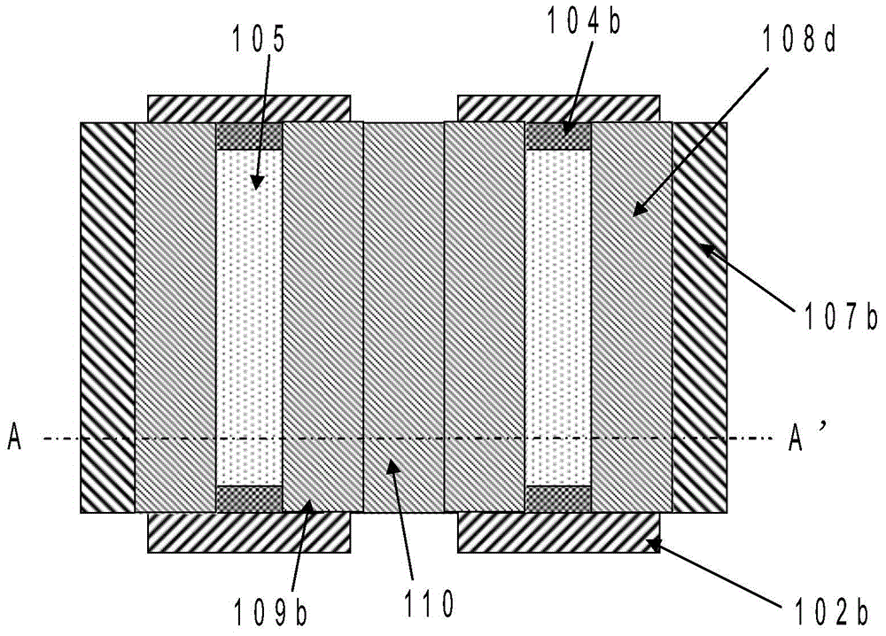
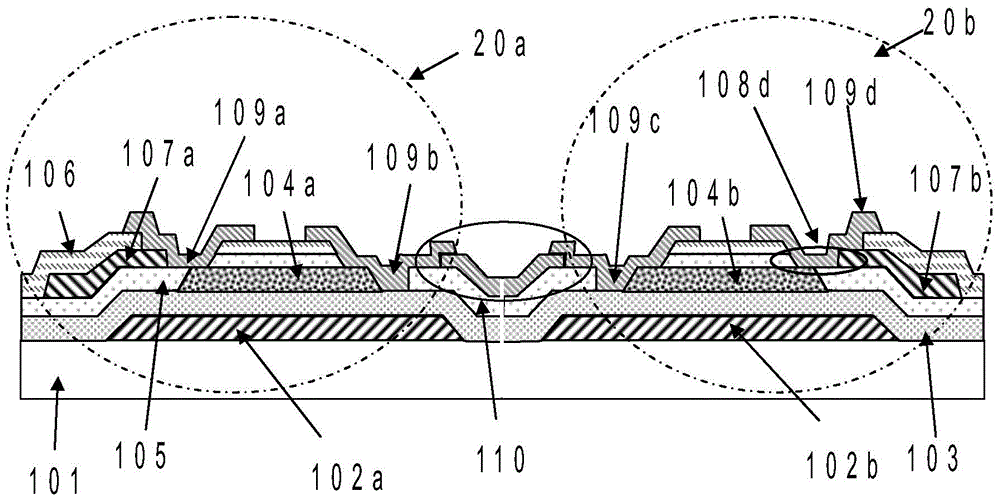
[0023] An embodiment of the present invention provides an array substrate, the structural diagram of the TFT in the gate drive circuit region of the array substrate can be as follows figure 2 as shown, image 3 for figure 2 The cross-sectional schematic diagram of the position of AA' in the middle, combined with the following figure 2 and image 3 The thin film transistor array substrate provided in this embodiment will be described.

[0024] In this embodim...


PUM


Abstract

The invention provides an array substrate comprising a display area and a drive circuit which is arranged around the display area. The drive circuit comprises multiple TFTs. At least one TFT comprises a first sub-TFT and a second sub-TFT. The first sub-TFT and the second sub-TFT are electrically connected via a first cross bridge. Material of the first cross bridge is transparent conductive material. A problem of poor solidification of frame-sealing glue, which is liable to occur when the grid electrode drive circuit is manufactured by adopting a thin film transistor, can be solved by the array substrate obtained by the scheme.

Description

technical field [0001] The invention relates to the field of flat panel display technology, in particular to an array substrate, a preparation method thereof, and a liquid crystal display panel. Background technique [0002] Such as figure 1 As shown, it is a schematic structural view of an existing display panel 1, including: a display area 10, a gate drive circuit 20 arranged around the display area 10, an IC circuit 30 below the display area 10, and glue on the gate drive circuit. Frame area (marked in the figure for clear display of the drawings), wherein, the display area 10 includes pixel units surrounded by a plurality of gates and a plurality of data lines, each pixel unit includes a pixel electrode, connected with a TFT ( Thin film transistor, thin film transistor) for switch control, and then display images. The driving circuit 20 also includes a plurality of TFTs, and each TFT is connected to a different gate or data line. Through the control of the TFT, the dri...

Claims


Application Information

Patent Timeline
Patent Type & Authority Applications(China)
IPC IPC(8): H01L27/12H01L21/77G02F1/133G02F1/1362G02F1/1368
CPCH01L27/1225H01L27/124H01L27/1259G02F1/13306H01L21/31111H01L21/47573H01L21/76802H01L27/1222H01L29/66765H01L29/66969H01L29/78669H01L29/7869
Inventor 曹兆铿楼均辉
Owner SHANGHAI TIANMA MICRO ELECTRONICS CO LTD
Why Eureka
Try Eureka