LED epitaxial layer growth method and LED epitaxial layer for increasing luminous efficiency

A growth method and luminous efficiency technology, applied in electrical components, circuits, semiconductor devices, etc., can solve the problems of easy leakage of electrons, hole consumption, and low injection efficiency, and achieve the effects of increasing luminous efficiency, increasing concentration, and improving injection

Active Publication Date: 2016-09-07
XIANGNENG HUALEI OPTOELECTRONICS
View PDF3 Cites 0 Cited by
  • Summary
  • Abstract
  • Description
  • Claims
  • Application Information

AI Technical Summary

Problems solved by technology

[0002] At present, the production of GaN-based LED blue-green light-emitting devices in China involves multiple quantum well layers formed by InGaN / GaN superlattice. The traditional quantum wells have flat energy bands, high electron concentration, and high mobility. The characteristics determine that the distribution of electrons in the quantum well is too much, and the disadvantage is that electrons are easy to leak to the P layer to consume holes, resulting in a decrease in the injection concentration of holes; the opposite characteristics of holes and electrons are low concentration, low mobility, and injection efficiency. Low

Method used


Image

  • LED epitaxial layer growth method and LED epitaxial layer for increasing luminous efficiency
  • LED epitaxial layer growth method and LED epitaxial layer for increasing luminous efficiency
  • LED epitaxial layer growth method and LED epitaxial layer for increasing luminous efficiency

Examples


Embodiment 1

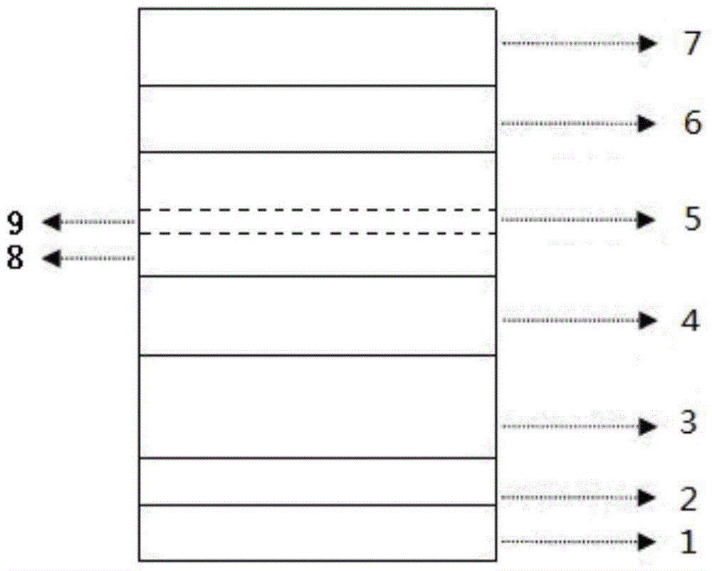
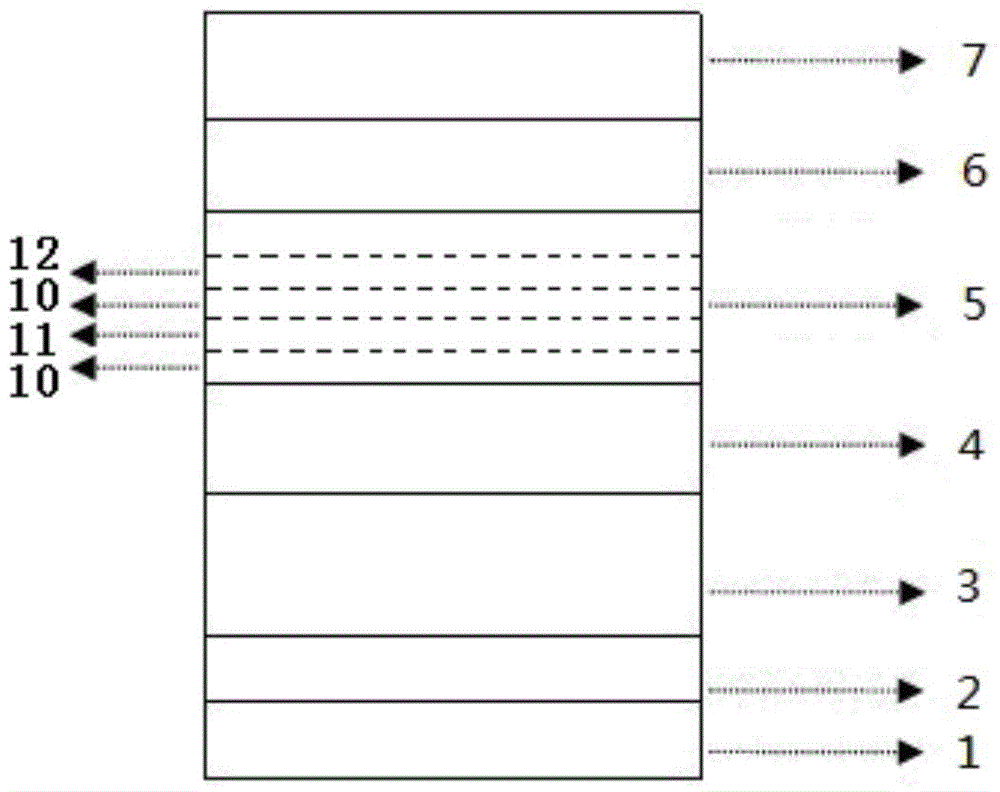
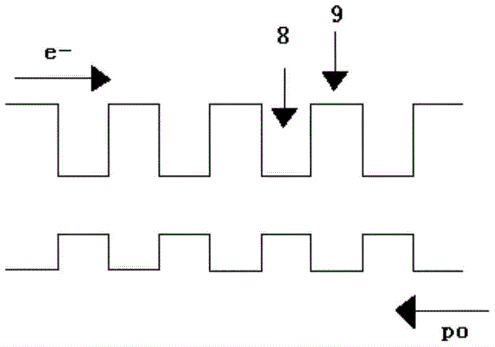
[0048] see figure 2 , the present invention uses Aixtron MOCVD to grow high-brightness GaN-based LED epitaxial wafers. Using high-purity H 2 or high purity N 2 or high purity H 2 and high purity N 2 The mixed gas as the carrier gas, high-purity NH 3 As the N source, the metal-organic source trimethylgallium (TMGa), triethylgallium (TEGa) is used as the gallium source, trimethylindium (TMIn) is used as the indium source, and the N-type dopant is silane (SiH 4 ), trimethylaluminum (TMAl) as the aluminum source, and the P-type dopant as magnesium dicene (CP 2 Mg), the substrate is (0001) sapphire, and the reaction pressure is between 100mbar and 800mbar.

[0049] A LED epitaxial layer growth method for increasing luminous efficiency, which sequentially includes processing a substrate, growing a low-temperature buffer GaN layer, growing a non-doped GaN layer, growing a Si-doped GaN layer, growing an active layer MQW, growing a P-type AlGaN layer, growing P-type GaN layer s...


PUM


Abstract

The invention provides an LED (Light Emitting Diode) epitaxial layer growing method capable of improving luminous efficiency and an LED epitaxial layer. An active layer MQW (Multiple Quantum Well) is grown through the steps that: a layer of InxGa1-xN and a layer of AlyGaN are grown, wherein x=0.15-0.25, y=0.10-0.15, and the cycle count of InxGa1-xN / AlyGa1-yN is 5-6; next, a layer of InxGa1-xN and a layer of InyGa1-yN are grown, wherein y=0.05-0.10, and the cycle count of InxGa1-xN / InyGa1-yN is 5-6. A quantum well barrier layer of a luminous layer is designed into a first InGaN / AlGaN superlattice and a combination offirst InGaN / second InGaN superlattices instead of a previous InGaN / GaN superlattice material, and therefore, the concentration of electrons and holes in the quantum well is increased and the luminous efficiency of the device is improved.

Description

technical field [0001] The invention relates to the technical field of LED epitaxial design, in particular to an LED epitaxial layer growth method for increasing luminous efficiency by combining InGaN / AlGaN superlattice and InGaN / InGaN superlattice and the obtained LED epitaxial layer. Background technique [0002] At present, the production of GaN-based LED blue-green light-emitting devices in China involves multiple quantum well layers formed by InGaN / GaN superlattice. The traditional quantum wells have flat energy bands, high electron concentration, and high mobility. The characteristics determine that the distribution of electrons in the quantum well is too much, and the disadvantage is that the electrons are easy to leak to the P layer to consume holes, resulting in a decrease in the injection concentration of holes; the opposite characteristics of holes and electrons are low concentration, low mobility, and injection efficiency. Low. Industry papers also pointed out t...

Claims


Application Information

Patent Timeline
Patent Type & Authority Patents(China)
IPC IPC(8): H01L33/00H01L33/06H01L33/30
CPCH01L33/007H01L33/0075H01L33/06H01L33/32
Inventor 林传强许孔祥周佐华
Owner XIANGNENG HUALEI OPTOELECTRONICS
Why Eureka
Try Eureka