Array substrate, manufacturing method thereof, liquid crystal display panel and liquid crystal display device

A technology of an array substrate and a manufacturing method, applied in the field of liquid crystal display, can solve the problem of large viewing angle deviation of liquid crystal displays, and achieve the effect of improving the large viewing angle deviation phenomenon

Active Publication Date: 2014-08-13
XIAMEN TIANMA MICRO ELECTRONICS +1
View PDF5 Cites 10 Cited by
  • Summary
  • Abstract
  • Description
  • Claims
  • Application Information

AI Technical Summary

Problems solved by technology

[0007] The object of the present invention is to provide an array substrate and its manufacturing method, a liquid crystal display panel and a liquid crystal display device, so as to solve the large viewing angle deviation phenomenon of the FFS mode liquid crystal display in the prior art

Method used


Image

  • Array substrate, manufacturing method thereof, liquid crystal display panel and liquid crystal display device
  • Array substrate, manufacturing method thereof, liquid crystal display panel and liquid crystal display device
  • Array substrate, manufacturing method thereof, liquid crystal display panel and liquid crystal display device

Examples


Embodiment 1

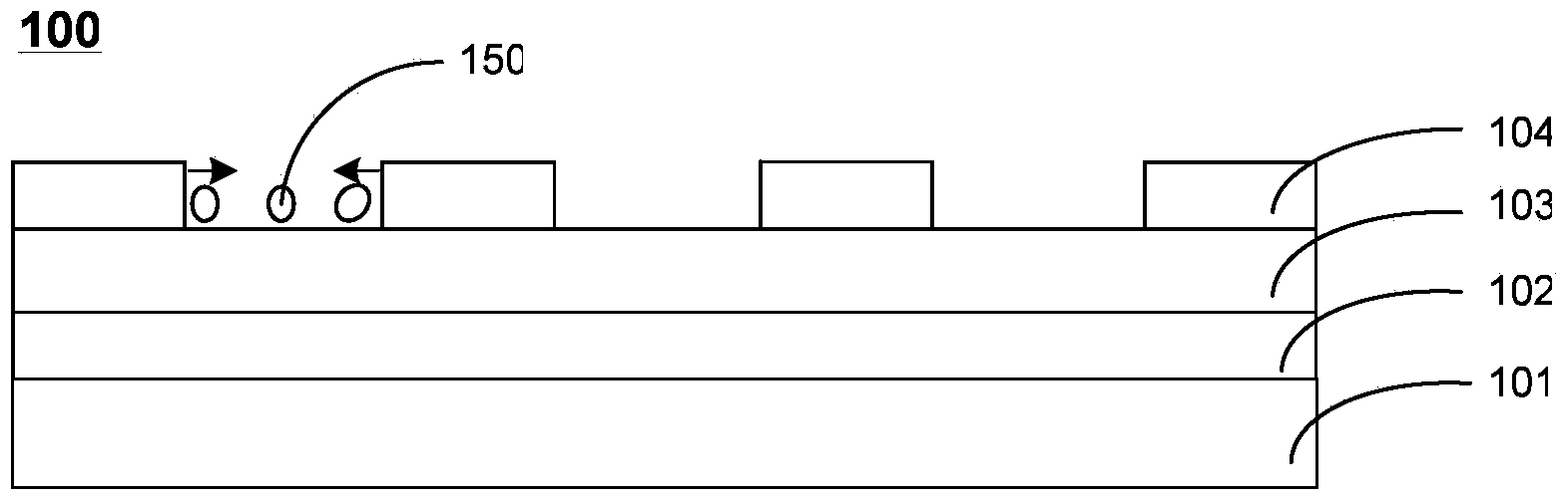
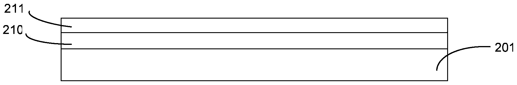
[0031] Please refer to Figure 3d , which is a partial structural diagram of the array substrate of the embodiment of the present invention. Such as Figure 3d As shown, the array substrate 200 includes: a base substrate 201 and a plurality of pixel units located on the base substrate 201, each pixel unit includes a first electrode 202, an insulating layer 203 and a second electrode stacked in sequence 204, a fringe field is formed between the first electrode 202 and the second electrode 202; wherein, the shape of the first electrode 202 is a sheet, and the second electrode 204 includes a plurality of strip electrodes, the The strip-shaped electrodes include at least one first strip-shaped sub-electrode 205 and at least one second strip-shaped sub-electrode 206, and the distance between the first strip-shaped sub-electrode 205 and the base substrate 201 is the same as that of the second strip-shaped sub-electrode 205. The distances between the electrodes 206 and the base sub...

Embodiment 2

[0053] Please refer to Figure 5d , which is a partial structural diagram of the array substrate of the embodiment of the present invention. Such as Figure 5d As shown, the array substrate 300 includes: a base substrate 301 and a plurality of pixel units located on the base substrate 301, each pixel unit includes a first electrode 302, an insulating layer 303 and a second electrode stacked in sequence 304, forming a fringe field between the first electrode 302 and the second electrode 302; wherein, the shape of the first electrode 302 is a sheet, and the second electrode 304 includes a plurality of strip electrodes, the The strip electrode includes at least one first strip sub-electrode 305 and at least one second strip sub-electrode 306, the distance between the first strip sub-electrode 305 and the base substrate 301 is the same as that of the second strip sub-electrode 305. The distances between the electrodes 306 and the base substrate 301 are not equal.

[0054] The d...

Embodiment 3

[0065] Please refer to Figure 7d , which is a partial structural diagram of the array substrate of the embodiment of the present invention. Such as Figure 7d As shown, the array substrate 400 includes: a base substrate 401 and a plurality of pixel units located on the base substrate 401, each pixel unit includes a first electrode 402, an insulating layer 403 and a second electrode stacked in sequence 404, a fringe field is formed between the first electrode 402 and the second electrode 402; wherein, the shape of the first electrode 402 is a sheet, and the second electrode 404 includes a plurality of strip electrodes, the The strip-shaped electrodes include at least one first strip-shaped sub-electrode 405 and at least one second strip-shaped sub-electrode 406, and the distance between the first strip-shaped sub-electrode 405 and the base substrate 401 is the same as that of the second strip-shaped sub-electrode 405. The distances between the electrodes 406 and the base sub...


PUM

PropertyMeasurementUnit
heightaaaaaaaaaa

Abstract

The invention relates to an array substrate, a manufacturing method of the array substrate, a liquid crystal display panel and a liquid crystal display device. The array substrate comprises a lining substrate and a plurality of pixel units located on the lining substrate, wherein each pixel unit comprises a first electrode, an insulating layer and a second electrode which are sequentially stacked, a fringing field is formed between the first electrode and the second electrode, the first electrode is sheet-shaped, the second electrode comprises a plurality of strip-shaped electrodes, the strip-shaped electrodes comprise at least one first strip-shaped sub-electrode and at least one second strip-shaped sub-electrode, and the distance of the first strip-shaped sub-electrode and the lining substrate is not equal to the distance of the second strip-shaped sub-electrode and the lining substrate. The high-low staggered second electrode is formed in the array substrate, the manufacturing method of the array substrate, the liquid crystal display panel and the liquid crystal display device, liquid crystal molecules can fully rotate, the compensation effect among the liquid crystal molecules is realized, and the large visual angle color error phenomenon can be improved.

Description

technical field [0001] The invention relates to the technical field of liquid crystal display, in particular to an array substrate and a manufacturing method thereof, a liquid crystal display panel and a liquid crystal display device. Background technique [0002] Currently, common liquid crystal display modes mainly include twisted nematic (TN) mode, vertical alignment (VA) mode and in-plane rotation mode. Among them, both the TN mode and the VA mode drive the liquid crystal molecules by applying an electric field between the upper and lower substrates, and electrodes are formed on the upper and lower substrates, which belongs to the longitudinal electric field drive. In the in-plane rotation mode, an electric field is applied on one side of the substrate to drive the liquid crystal molecules, and only one side of the substrate is provided with electrodes, which belongs to the transverse electric field drive. The liquid crystal molecules driven by the transverse electric f...

Claims


Application Information

Patent Timeline
Patent Type & Authority Applications(China)
IPC IPC(8): G02F1/1343G02F1/1333
Inventor 林友道沈柏平宋琼
Owner XIAMEN TIANMA MICRO ELECTRONICS
Why Eureka
Try Eureka