
Ldmos device with double-sloped field plate

A field plate and slope technology, applied in semiconductor devices, semiconductor/solid-state device manufacturing, electrical components, etc., can solve the problem of unusable transistors

Active Publication Date: 2014-08-20
FAIRCHILD SEMICON CORP
View PDF4 Cites 9 Cited by
  • Summary
  • Abstract
  • Description
  • Claims
  • Application Information

AI Technical Summary

Problems solved by technology

As performance requirements for semiconductor devices increase, producing transistors with acceptable Rdson values ​​and acceptable breakdown voltage values ​​may not be achievable using current methods

Method used


Image

  • Ldmos device with double-sloped field plate
  • Ldmos device with double-sloped field plate
  • Ldmos device with double-sloped field plate

Examples


Embodiment Construction

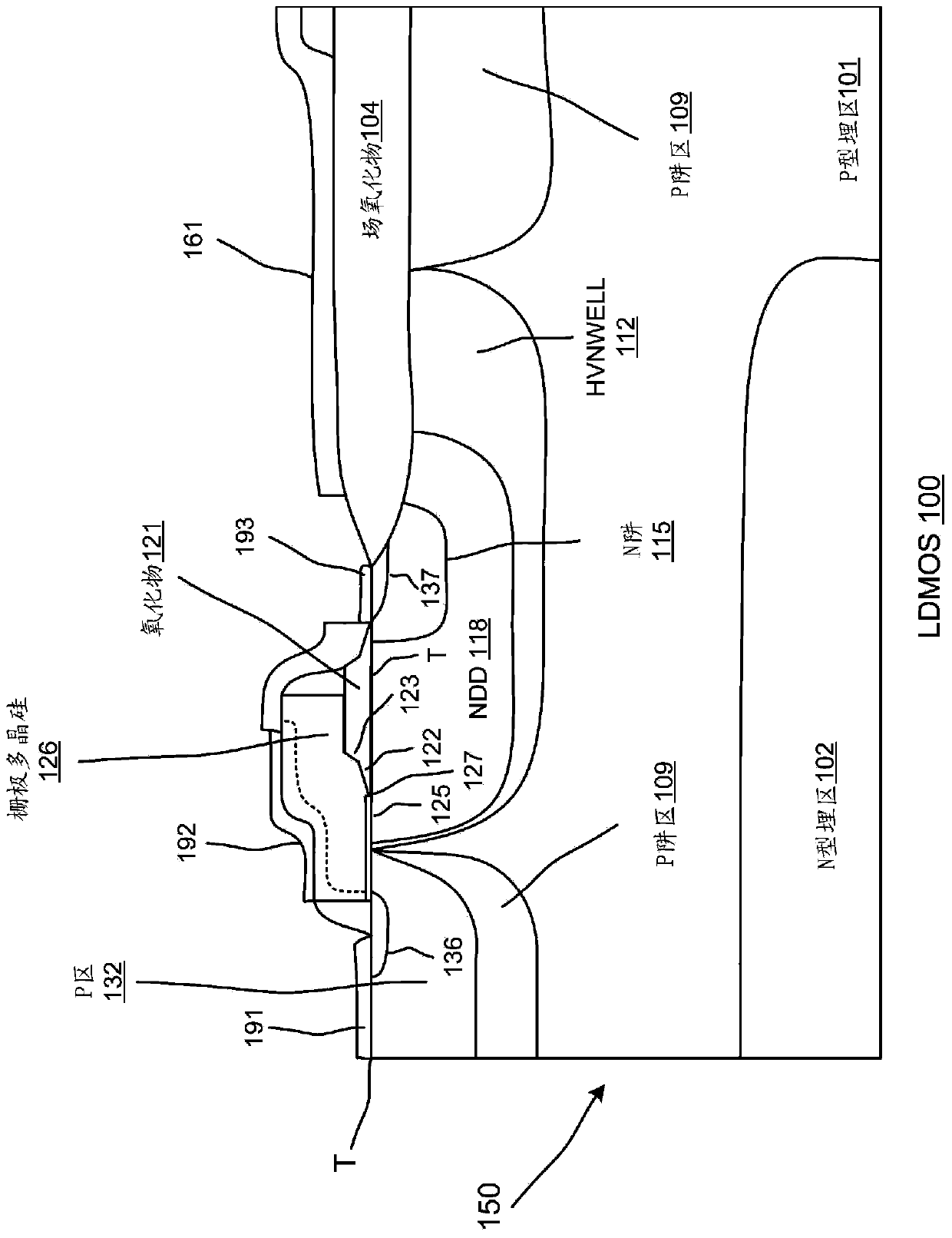
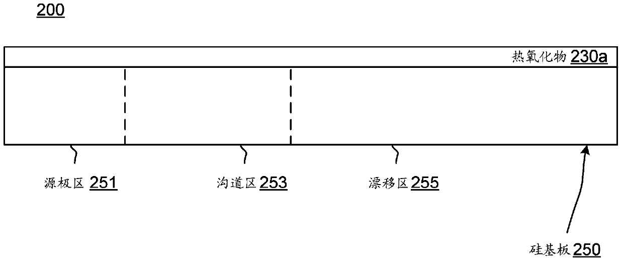
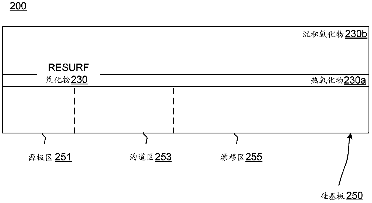
[0012] The disclosure herein relates to semiconductor devices, such as laterally diffused metal-oxide-semiconductor (LDMOS) transistors, having double-slope field plates (which may also be referred to as field dielectric plates or drift field dielectrics). The disclosure herein also relates to corresponding methods for producing such semiconductor devices. Such LDMOS devices with double sloped field plates can be produced with increased drift dose (to lower Rdson), while also having similar or improved breakdown voltage performance.

[0013] Furthermore, by using the semiconductor processing methods described herein, one or more process steps in a semiconductor process that overlap or correspond to one or more process steps used to produce other semiconductor devices (eg, LDMOS transistors) can be used to produce Semiconductor devices (eg, other than LDMOS transistors). For example, a process step used to produce a portion of a first semiconductor device may also be used to ...


PUM


Abstract

In one general aspect, an apparatus can include a channel region disposed in a semiconductor substrate, a gate dielectric disposed on the channel region and a drift region disposed in the semiconductor substrate adjacent to the channel region. The apparatus can further include a field plate having an end portion disposed between a top surface of the semiconductor substrate and the gate dielectric The end portion can include a surface in contact with the gate dielectric, the surface having a first portion aligned along a first plane non-parallel to a second plane along which a second portion of the surface is aligned, the first plane being non-parallel to the top surface of the semiconductor substrate and the second plane being non-parallel to the top surface of the semiconductor substrate.

Description

technical field [0001] This specification relates to laterally diffused metal oxide semiconductor transistors and methods of forming the same. Background technique [0002] Designing and engineering transistors for production using semiconductor processes typically involves trade-offs of one or more performance parameters with one or more other performance parameters. Such performance parameters may include drain-source on-resistance (Rdson), off-breakdown voltage (BVoff), and on-breakdown voltage (BVon), as some examples. For example, in laterally diffused metal-oxide-semiconductor (LDMOS) transistors, the dopant dose in the drift region (drift dose or DD) can be altered to vary the Rdson of a given LDMOS transistor. For example, increasing the drift dose of the semiconductor process used to produce a given LDMOS transistor will reduce the Rdson of that transistor compared to an LDMOS transistor of the same physical configuration produced using a lower drift dose. [0003...

Claims


Application Information

Patent Timeline
IPC IPC(8): H01L29/78H01L29/40H01L21/336
CPCH01L29/7816H01L29/66681H01L29/402H01L29/404H01L21/31111H01L29/0847H01L29/1045H01L29/1083H01L29/42368H01L29/456H01L29/4933H01L29/665H01L29/66659H01L29/7835H01L29/7823
Inventor 金成龙马克·施密特克里斯托弗·纳萨尔史蒂文·莱比格尔
Owner FAIRCHILD SEMICON CORP
Learn More