Supercharge Your Innovation With Domain-Expert AI Agents!

An erbium-doped zinc nitride thin-film optical waveguide and its preparation method

A zinc nitride and optical waveguide technology, applied in the direction of optical waveguide light guide, light guide, optics, etc., can solve the problems of optical waveguide that cannot obtain luminous efficiency, low refractive index of erbium-doped zinc nitride film, and poor range distribution shape, etc., to achieve Improved luminous efficiency, low cost, and low energy

Inactive Publication Date: 2016-04-06
SHANDONG JIANZHU UNIV
View PDF1 Cites 0 Cited by
  • Summary
  • Abstract
  • Description
  • Claims
  • Application Information

AI Technical Summary

Problems solved by technology

However, when the inventors adopted the erbium-doped zinc nitride optical waveguide prepared by the method disclosed in the reference document 1 according to the technical inspiration of the reference document 1, they found the following problem: the obtained erbium-doped zinc nitride film contained a large amount of zinc oxide , In addition, the erbium ions are too dispersed in the zinc nitride film layer, and the range distribution is poor; thus the refractive index of the erbium-doped zinc nitride film is too low, and a channel with high efficiency cannot be formed; an optical waveguide with high luminous efficiency cannot be obtained

Method used


Image

  • An erbium-doped zinc nitride thin-film optical waveguide and its preparation method
  • An erbium-doped zinc nitride thin-film optical waveguide and its preparation method
  • An erbium-doped zinc nitride thin-film optical waveguide and its preparation method

Examples


Embodiment 1

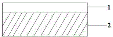
[0028] (1) Zinc nitride film 1 on quartz glass substrate 2 (such as figure 1 shown) to perform optical surface polishing, cleaning and drying; wherein, the thickness of the zinc nitride film 1 is 100-800nm;

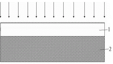
[0029] (2) Put the processed zinc nitride film into the accelerator target chamber and pump it to 10 -4 The background vacuum of Pa, using erbium ions as implanted ions, carries out the process of implanting erbium ions into zinc nitride thin films (such as figure 2 shown); adjust the irradiation energy to 500KeV, and the implant dose to 5×10 15 ions / cm 2 , the beam density is 0.5μA / cm 2 , the angle between the normal direction of the surface of the zinc nitride film and the direction of the incident ion beam is 7°; the sample of erbium-doped zinc nitride film 3 is obtained;

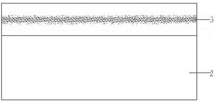
[0030] (3) Place the sample of erbium-doped zinc nitride thin film 3 in a nitriding furnace for annealing to obtain an erbium-doped zinc nitride thin film optical waveguide 4; wherein, the anne...

Embodiment 2-9

[0033] The operation steps are the same as in Example 1, and the involved parameters "irradiation energy, implant dose, angle, annealing temperature, and nitrogen gas volume" are shown in Table 1;

[0034] Table 1:

[0035]

A

B

angle

C

D

E

F

G

Example 2

300

5×10 15

400

500

50-130

31%

12%

Example 3

600

5×10 15

400

500

120-200

32%

11%

Example 4

500

10 14

400

500

100-170

38%

9%

Example 5

500

10 16

400

500

80-170

29%

8%

Example 6

500

5×10 15

300

500

110-190

24%

10%

Example 7

500

5×10 15

800

500

100-180

45%

5%

Example 8

500

5×10 15

800

300

80-200

44%

4%

Example 9

500

5×10 15

800

600

90-190

45%

6%

[0036]...


PUM

PropertyMeasurementUnit
thicknessaaaaaaaaaa
depthaaaaaaaaaa

Abstract

The invention relates to a preparation method for semiconductor material optical waveguide, in particular to an erbium-doped zinc nitride thin film optical waveguide and a preparation method. Erbium ions are tried to be doped to a novel zinc nitride semiconductor material thin film layer for the first time, the fact that the erbium-doped zinc nitride optical waveguide is prepared through the ion irradiation technology is proved to be feasible, and the zinc nitride optical waveguide is promoted greatly. In the erbium ion irradiation zinc nitride thin film process, irradiation energy is 300-600 KeV, implantation dose is 1014-1016 ions / cm <2>, and beam current density is 0.3-0.8 micron A / cm <2>; the included angle between the zinc nitride thin film surface normal direction and ion beam incident direction is 7 degrees; annealing treatment is carried out on erbium-doped zinc nitride thin film samples in nitrogen in a nitriding furnace. No zinc oxide is mixed in the zinc nitride thin optical waveguide prepared through the method, and purity is high. Erbium ions are distributed in a Gaussian distribution mode, erbium ions with the maximum concentration are concentrated in the middle of a thin film, luminous efficiency is remarkably improved, and fluorescence intensity gains are increased by 4-15 percent.

Description

technical field [0001] The invention relates to a method for preparing a semiconductor material optical waveguide, in particular to an erbium-doped zinc nitride film optical waveguide and its preparation method. Background technique [0002] Optical waveguide is a basic unit in the research field of modern integrated optics, which regulates the channel in the direction of light wave propagation. Optical waveguides play a central and important role in modern optical communications because of their excellent performance, high integration, and low manufacturing cost. Optical waveguides are widely used, mainly waveguide lasers and waveguide frequency doublers, waveguide amplifiers, optical path converters, polarizers, waveguide splitters, couplers, modulators, wavelength division multiplexers and demultiplexers, etc. Due to the important existence value of optical waveguides, researchers have been exploring various methods to prepare optical waveguides on different materials. ...

Claims


Application Information

Patent Timeline
Patent Type & Authority Patents(China)
IPC IPC(8): G02B6/134G02B6/122G02B6/13
Inventor 王凤翔孙舒宁付刚陈志华李双
Owner SHANDONG JIANZHU UNIV
Features
  • R&D
  • Intellectual Property
  • Life Sciences
  • Materials
  • Tech Scout
  • Unparalleled Data Quality
  • Higher Quality Content
  • 60% Fewer Hallucinations
Learn More